Opto-electronic apparatus and manufacturing method thereof

a manufacturing method and optoelectronic technology, applied in the field of optoelectronic devices, can solve the problems of inability to manufacture display panels that are manufactured, micro leds may easily have interference with other components configured, and poor quality of manufactured display panels, so as to reduce the damage of components due to undesired collisions and interferences, improve manufacturing yield, and reduce manufacturing time

Active Publication Date: 2017-06-15
LG DISPLAY CO LTD
View PDF0 Cites 10 Cited by
  • Summary
  • Abstract
  • Description
  • Claims
  • Application Information

AI Technical Summary

Benefits of technology

[0030]As mentioned above, the opto-electronic apparatus and manufacturing method thereof of the invention configure the protrusions on the substrate with a height design corresponding to other components, so that the collisions and interferences between the opto-electronic units and other components disposed on the substrate can be avoided during the transfer step of the opto-electronic units. Thus, the damages of the components due to the undesired collisions and interferences can be reduced. Accordingly, the manufacturing time can be shortened, the manufacturing yield can be improved, and the manufacturing cost can be decreased.

Problems solved by technology

Accordingly, the manufacturing time and cost utilizing the micro LED are increased.
If directly using a pick-up head to grab a plurality of micro LEDs from the carrier and transfer them to the matrix substrate, the micro LEDs may easily have interferences with other components configured on the matrix substrate due to the fine size of the micro LEDs.
These undesired interferences can cause the poor quality of the manufactured display panel, and will increase the cost in the later inspection and repair procedures.

Method used


Image

  • Opto-electronic apparatus and manufacturing method thereof
  • Opto-electronic apparatus and manufacturing method thereof
  • Opto-electronic apparatus and manufacturing method thereof

Examples


Embodiment Construction

[0052]The present invention will be apparent from the following detailed description, which proceeds with reference to the accompanying drawings, wherein the same references relate to the same elements.

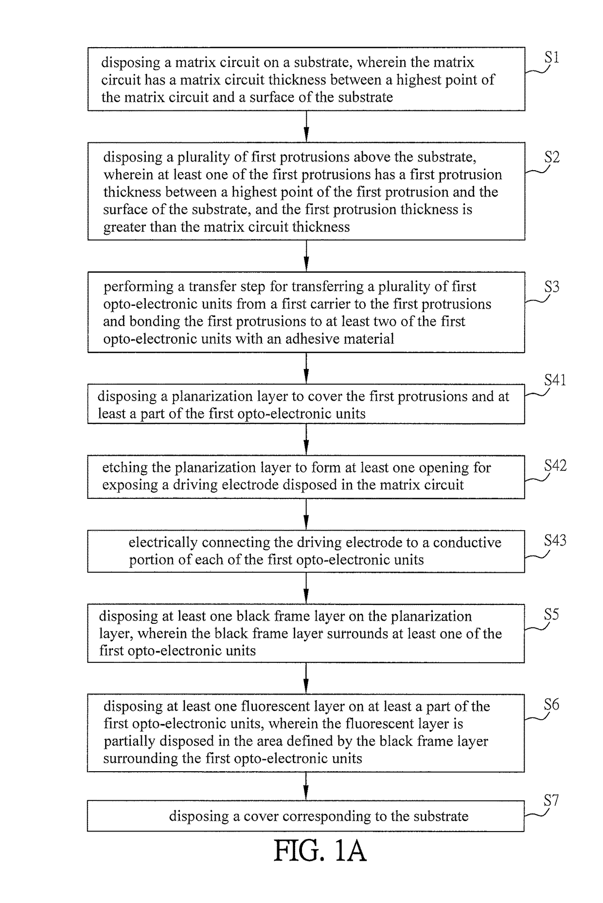
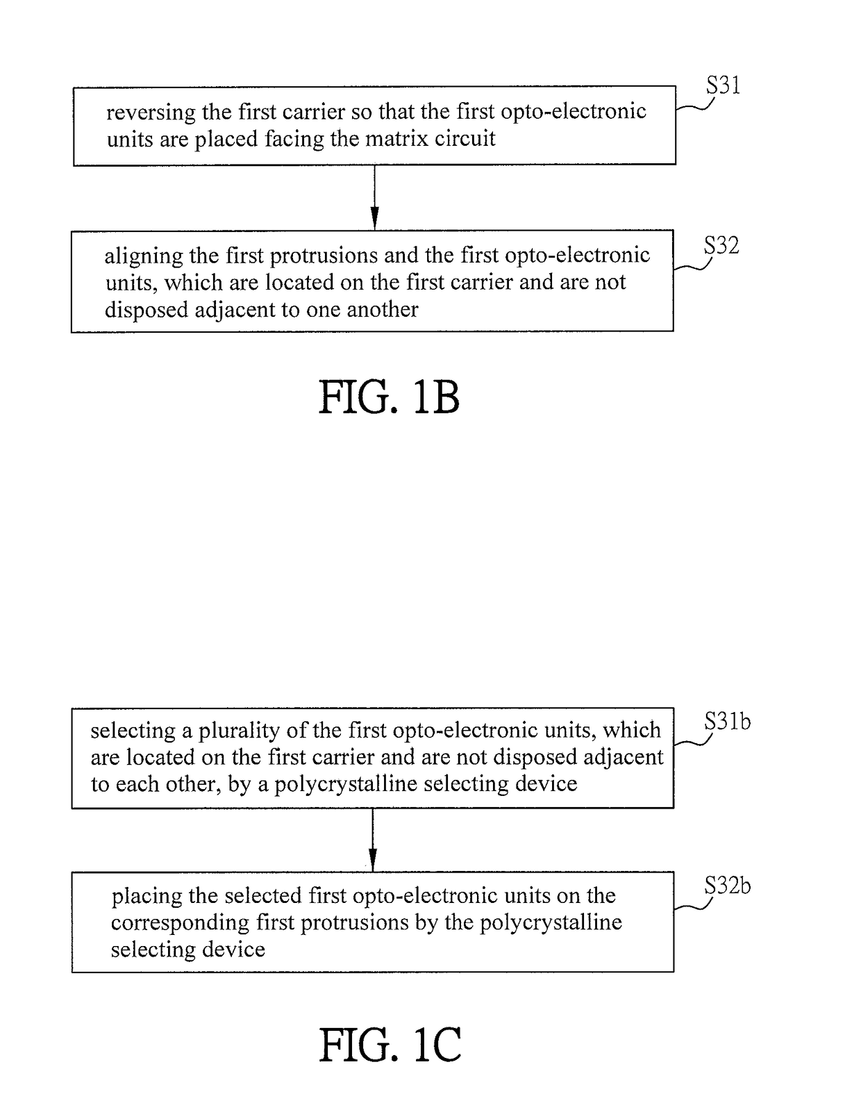
[0053]FIG. 1A is a flow chart of a manufacturing method of an opto-electronic apparatus according to an embodiment of the invention. The opto-electronic apparatus in the following embodiments can be a display panel, a multimedia board, a sensing apparatus, a semiconductor apparatus or an illumination apparatus, and this invention is not limited. The manufacturing method of an opto-electronic apparatus of the embodiment includes the following steps.

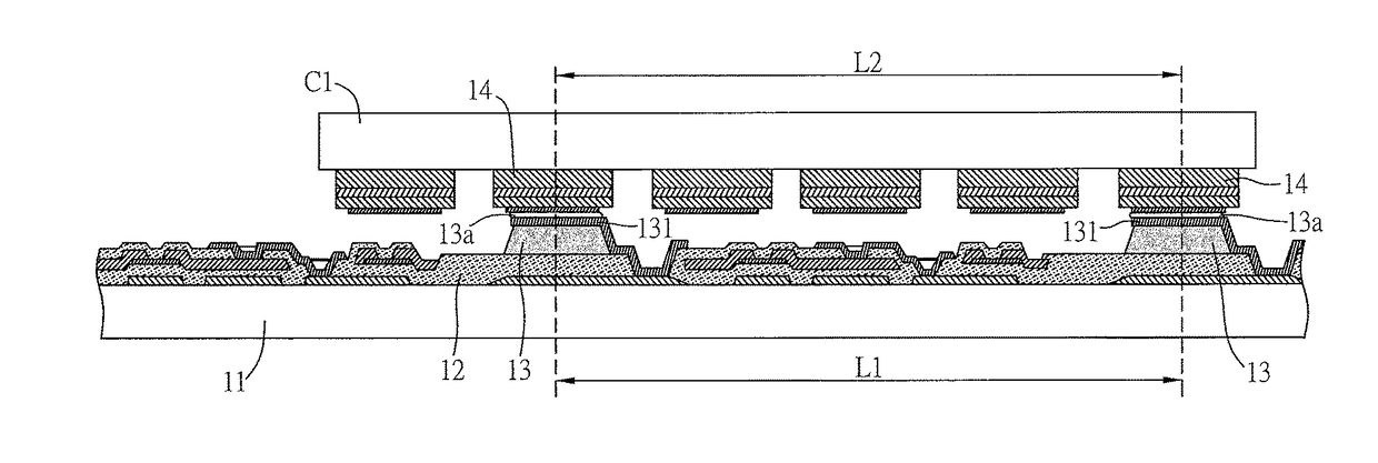
[0054]FIG. 2A is a schematic diagram showing the configurations of the substrate and the matrix circuit in the manufacturing method of an opto-electronic apparatus according to the embodiment of the invention. Referring to FIG. 1A in view of FIG. 2A, the step S1 is to dispose a matrix circuit 12 above a substrate 11, wherein the matrix circu...


PUM


Abstract

An opto-electronic apparatus and a manufacturing method thereof are disclosed. The manufacturing method of the opto-electronic apparatus includes the following steps of: disposing a matrix circuit on a substrate, wherein the matrix circuit has a matrix circuit thickness between the highest point of the matrix circuit and the surface of the substrate; disposing a plurality of first protrusions above the substrate, wherein at least one of the first protrusions has a first protrusion thickness between the highest point of the first protrusion and the surface of the substrate, and the first protrusion thickness is greater than the matrix circuit thickness; and performing a transfer step for transferring a plurality of first opto-electronic units from a first carrier to the first protrusions and bonding the first protrusions to at least two of the first opto-electronic units with an adhesive material.

Description

CROSS REFERENCE TO RELATED APPLICATIONS[0001]This Non-provisional application claims priority under 35 U.S.C. §119(a) on Patent Application No(s). 104142149 filed in Taiwan, Republic of China on Dec. 15, 2015, the entire contents of which are hereby incorporated by reference.BACKGROUND OF THE INVENTIONField of Invention[0002]The present invention relates to an electronic apparatus and, in particular, to an opto-electronic apparatus and a manufacturing method thereof.Related Art[0003]Recently, the micro LED array display device composed of micro LEDs (μLED) has been developed. Compared to the conventional LED display device, the micro LED array display device does not need additional backlight source, so that it can be easily manufactured with light weight and thinner size. Compared to the self-illumination OLED display device, the micro LED array display device is more stable and reliable, and does not have the image sticking issue. In addition, the micro LED can be widely applied t...

Claims


Application Information

Patent Timeline
Patent Type & Authority Applications(United States)
IPC IPC(8): H01L25/00H01L23/00H01L25/16H01L33/62H01L27/12
CPCH01L25/50H01L2924/1426H01L27/1248H01L27/1262H01L25/167H01L24/97H01L24/83H01L2933/0066H01L2224/95001H01L2224/95136H01L2224/83851H01L2924/0781H01L2224/83951H01L2224/83139H01L2924/1515H01L2924/12041H01L33/62G09F9/33G09G3/32H01L21/67144H01L27/156
Inventor YEN, YUNG-YU
Owner LG DISPLAY CO LTD
Why Eureka
Try Eureka