Method of Forming a Feature of a Target Material on a Substrate

Active Publication Date: 2017-06-22
INTERUNIVERSITAIR MICRO ELECTRONICS CENT (IMEC VZW) +1
View PDF3 Cites 4 Cited by
  • Summary
  • Abstract
  • Description
  • Claims
  • Application Information

AI Technical Summary

Benefits of technology

[0027]According to one embodiment, the feature of the sacrificial material can be formed on a buffer layer of the substrate which is inert to the precursor(s) of the deposition process. The buffer layer may hence prevent underlying materials from reacting with the precursors of the deposition process.
[0028]Accordin

Problems solved by technology

A drawback with this technique is however that the etchants may react with the material that is patterned in such a way that the electronic properties of the material are adversely affected at the edges of

Method used


Image

  • Method of Forming a Feature of a Target Material on a Substrate
  • Method of Forming a Feature of a Target Material on a Substrate
  • Method of Forming a Feature of a Target Material on a Substrate

Examples


Embodiment Construction

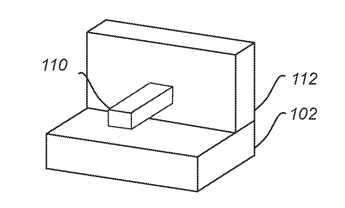
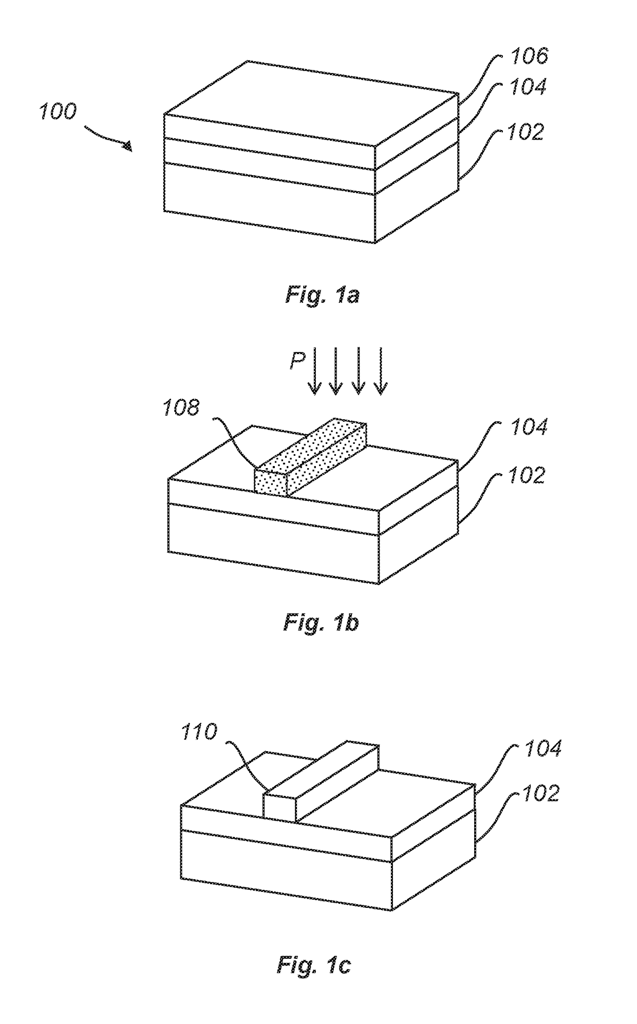
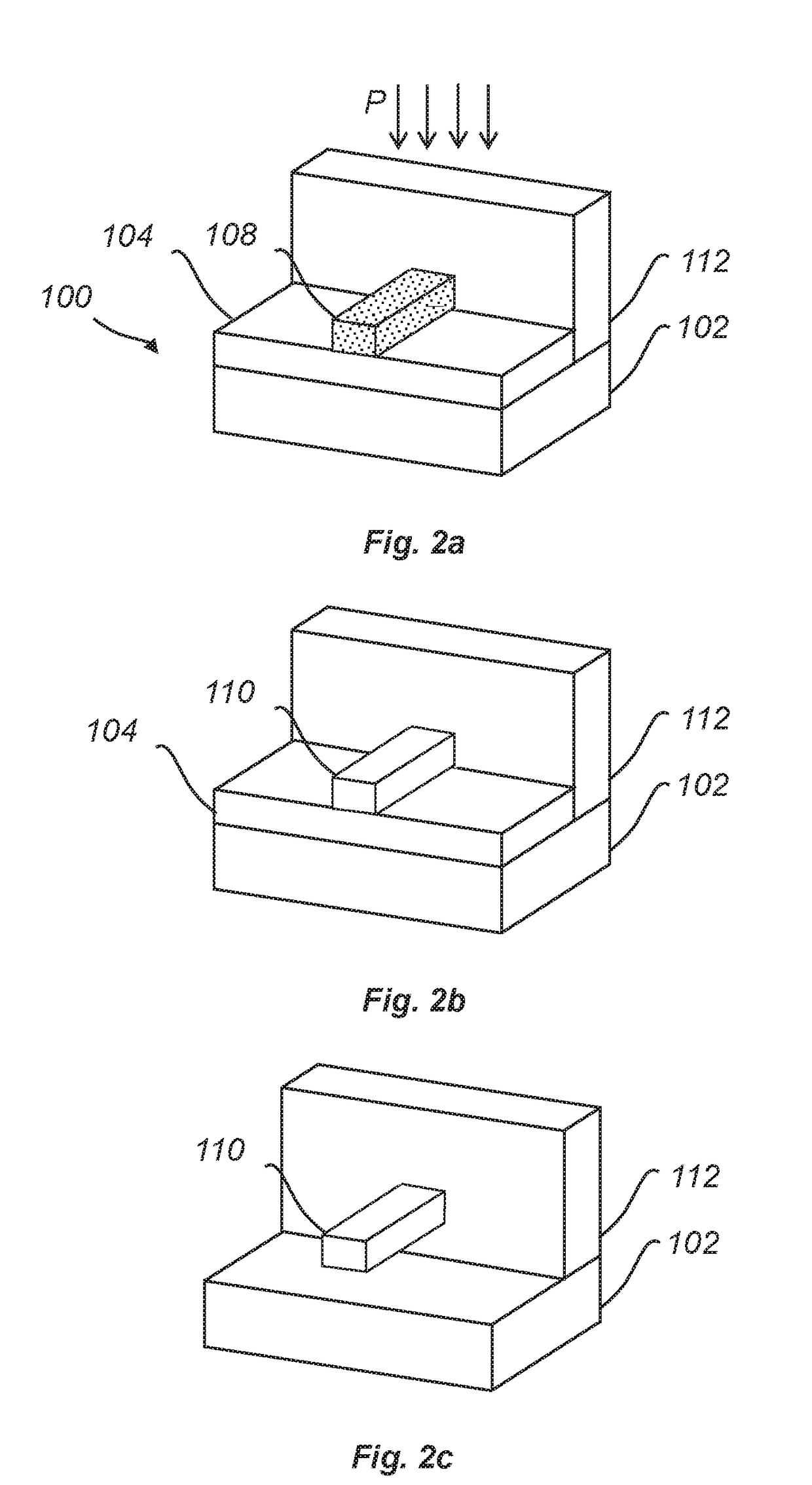
[0073]FIGS. 1a-c schematically illustrates a method of forming a feature 110 of a target material on a substrate 100.

[0074]FIG. 1a illustrates a stack of layers which in a bottom-up direction include a substrate layer 102, a buffer layer 104 and a sacrificial material layer 106. The substrate layer 102 and the buffer layer 104 form the substrate 100 on which the feature 110 will be formed, in accordance with the following.

[0075]It may be noted that FIG. 1a only shows a portion of the substrate 100 and that the substrate 100 may extend horizontally / laterally beyond the portion shown in FIG. 1a.

[0076]According to the method, the sacrificial material layer 106 can be patterned to form a feature of the sacrificial material 108 which is shown in FIG. 1b. The feature 108 may be formed by patterning the sacrificial material layer 106 using a lithography and etching process. The feature 108 may also be directly formed on the substrate 100 using an atomic layer deposition (ALD) process.

[007...


PUM


Abstract

A method is provided for forming a feature of a target material on a substrate. The method including:
    • forming a feature of a sacrificial material on the substrate; and
    • forming the feature of the target material by a deposition process during which the feature of the sacrificial material is removed from the substrate by forming a volatile reaction product with a precursor of the deposition process, wherein the sacrificial material is replaced by the target material and the target material is selectively deposited on surface portions of the substrate, which portions were covered by the feature of the sacrificial material, to form the feature of the target material.

Description

CROSS-REFERENCE[0001]This application claims priority from EP 15201632.5 filed Dec. 21, 2015, which is incorporated by reference in its entirety.TECHNICAL FIELD[0002]The present disclosure relates to a method of forming a feature of a target material on a substrate.BACKGROUND[0003]In semiconductor device manufacturing, forming features on the substrate is frequently required wherein the shape and dimension of the feature depends on the type of device that is to be manufactured. One standard technique for forming features involves patterning a material layer using, for instance a combination of lithography and etching. A drawback with this technique is however that the etchants may react with the material that is patterned in such a way that the electronic properties of the material are adversely affected at the edges of the features (i.e. the boundary surfaces of the features which are formed during the etching). This drawback may be more pronounced as device dimensions, and thus th...

Claims


Application Information

Patent Timeline
IPC IPC(8): H01L21/02
CPCH01L21/02645H01L21/02568H01L21/02603H01L21/02205H01L21/0226H01L21/02614H01L21/02658
Inventor DELABIE, ANNELIESHEYNE, MARKUS
Owner INTERUNIVERSITAIR MICRO ELECTRONICS CENT (IMEC VZW)
Why Eureka
Try Eureka