Atomic layer deposition of iii-v compounds to form v-nand devices

a technology of atomic layer deposition and v-nand, which is applied in the direction of semiconductor devices, basic electric elements, electrical equipment, etc., can solve the problems of high manufacturing cost, long time-consuming and labor-intensive, and inability to fabricate single crystalline channels in v-nand channels

Active Publication Date: 2017-06-29
ASM IP HLDG BV
View PDF6 Cites 296 Cited by
  • Summary
  • Abstract
  • Description
  • Claims
  • Application Information

AI Technical Summary

Problems solved by technology

In addition, other factors potentially affecting the conductivity of the poly-silicon channel include the intrinsic mobility of electrons in silicon and the resistance induced by the grain boundaries in poly-silicon.

Method used


Image

  • Atomic layer deposition of iii-v compounds to form v-nand devices
  • Atomic layer deposition of iii-v compounds to form v-nand devices
  • Atomic layer deposition of iii-v compounds to form v-nand devices

Examples


Embodiment Construction

[0023]Although certain embodiments and examples are disclosed below, it will be understood by those in the art that the invention extends beyond the specifically disclosed embodiments and / or uses of the invention and obvious modifications and equivalents thereof. Thus, it is intended that the scope of the invention disclosed should not be limited by the particular disclosed embodiments described below.

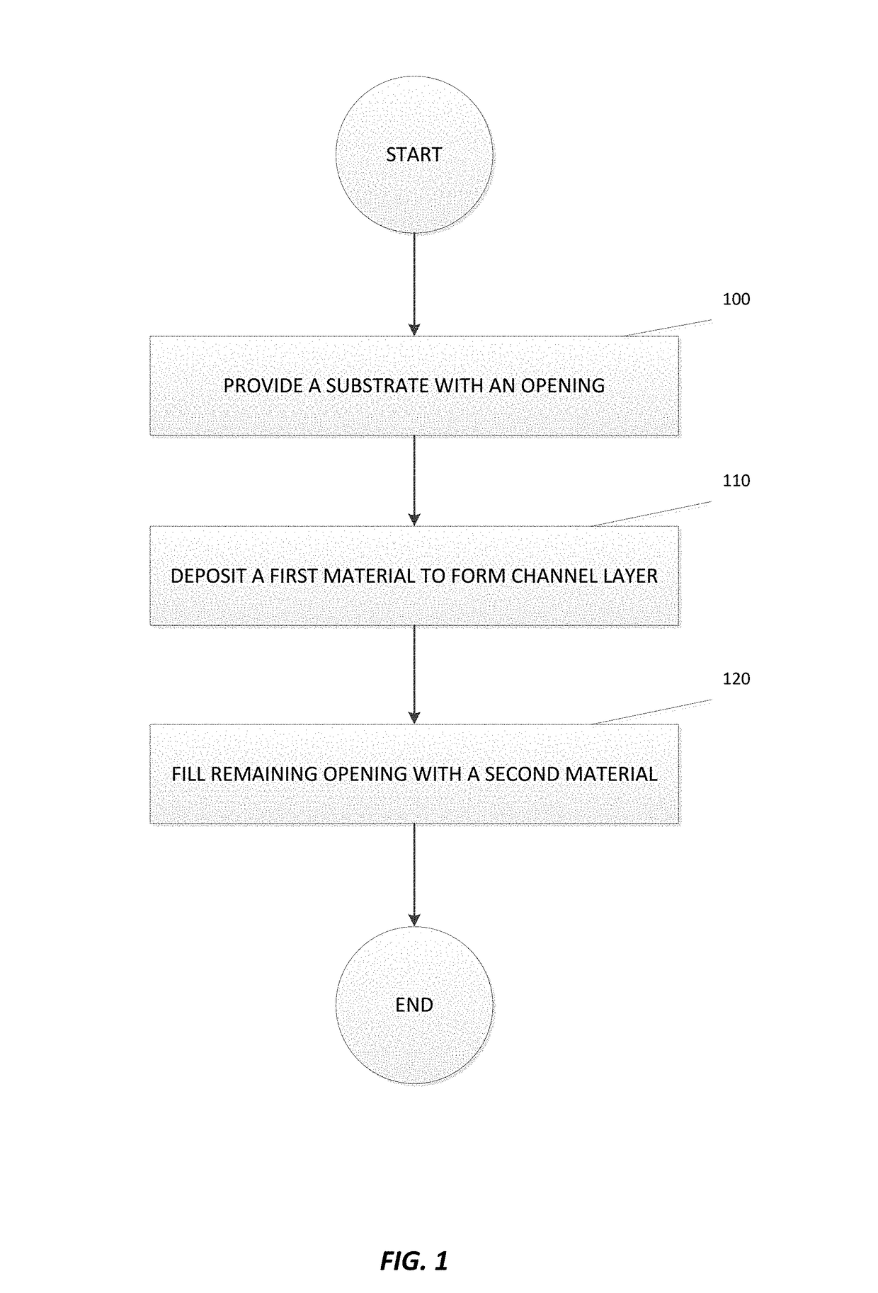
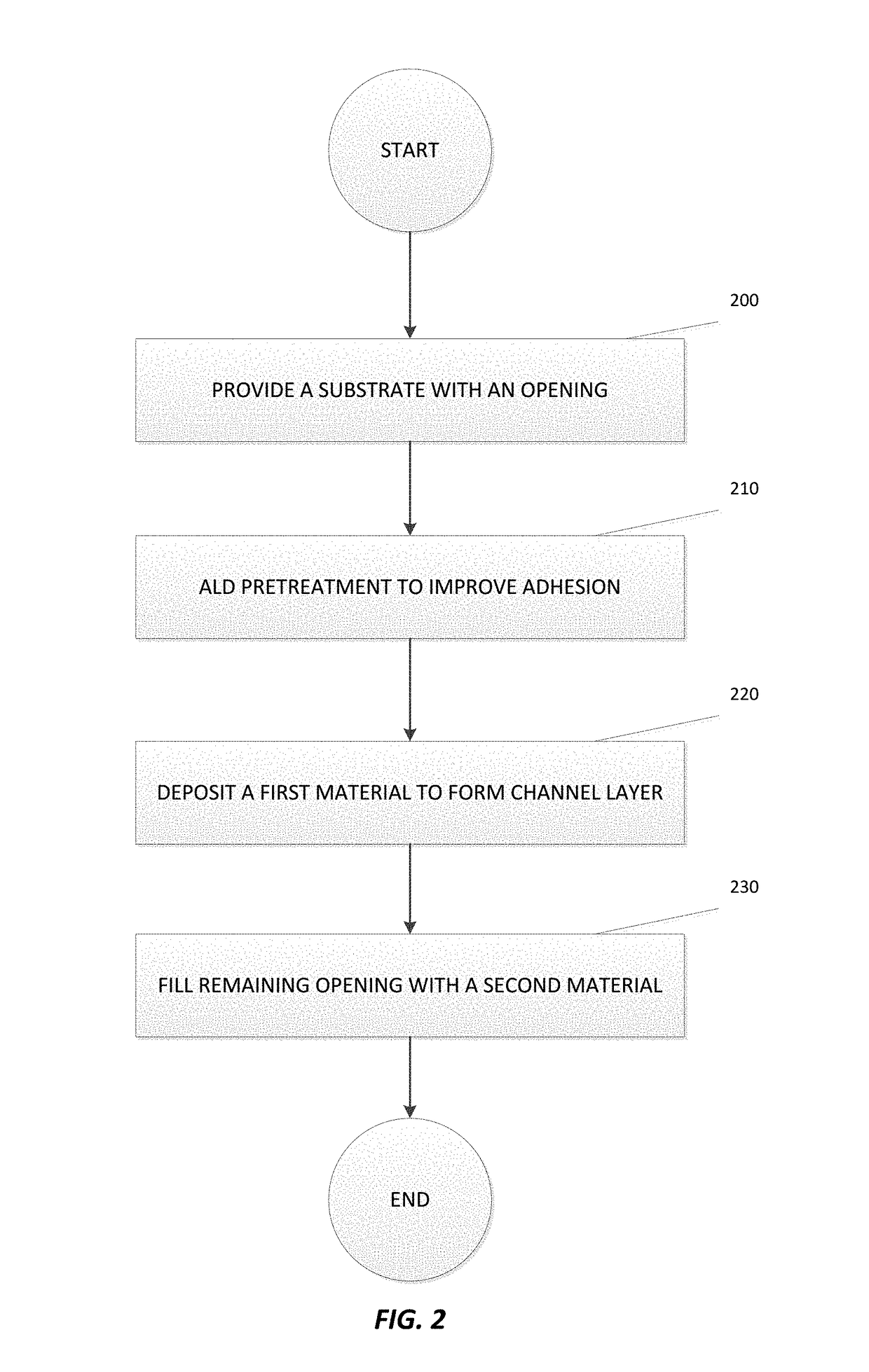
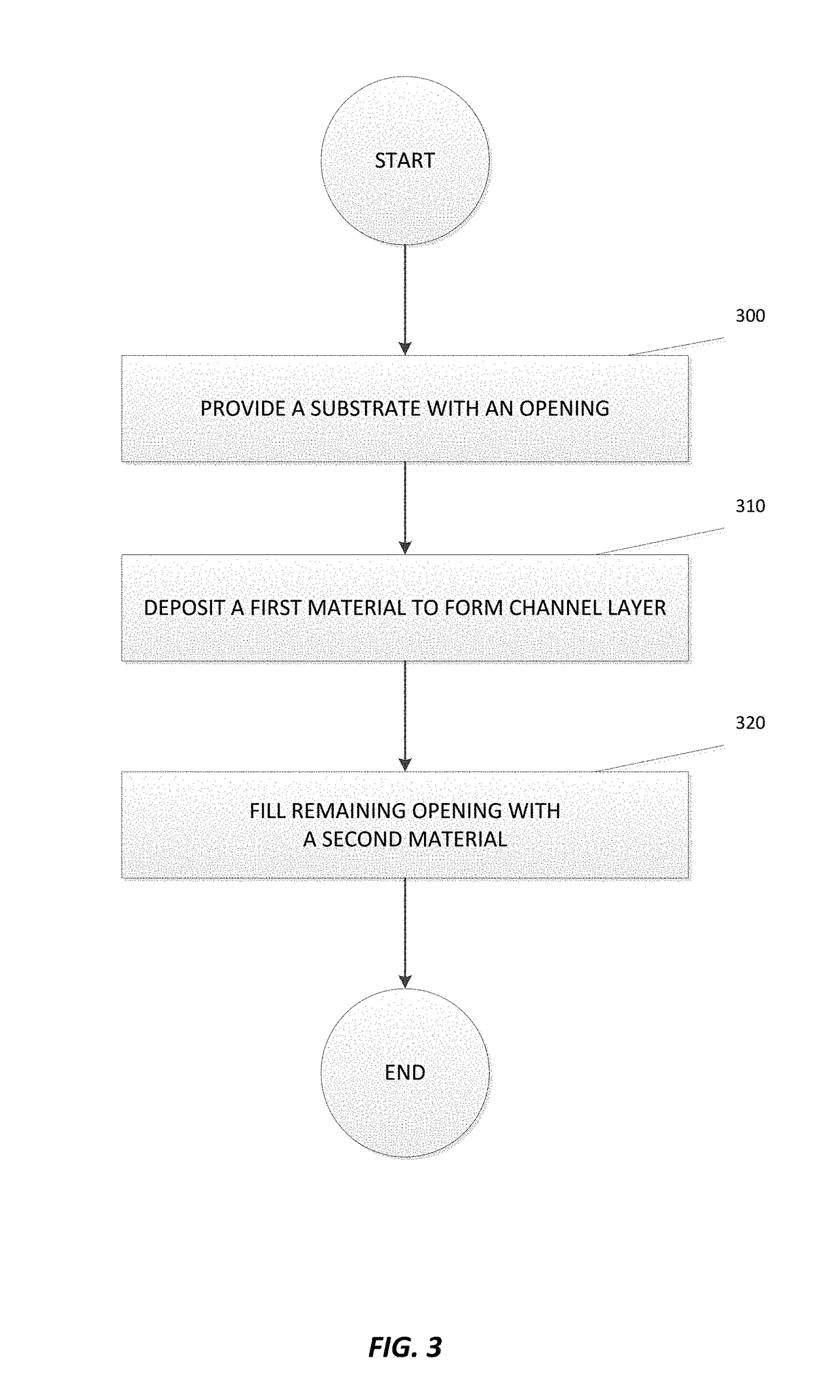
[0024]Embodiments of the invention relate to methods of manufacturing or treating a V-NAND device. Specifically, the methods include manufacturing a channel material or treating the channel material in order to allow for optimum performance and stability. Embodiments of the invention may take place in in batch, mini-batch, or single-wafer reactors.

[0025]FIG. 1 illustrates one method in accordance with the invention. The method includes a step of providing a substrate 100. The substrate of the providing step 100 has an opening that may be formed by etching, for example. The opening of t...


PUM


Abstract

A method for forming a V-NAND device is disclosed. Specifically, the method involves deposition of at least one of semiconductive material, conductive material, or dielectric material to form a channel for the V-NAND device. In addition, the method may involve a pretreatment step where ALD, CVD, or other cyclical deposition processes may be used to improve adhesion of the material in the channel.

Description

CROSS REFERENCE TO RELATED APPLICATION[0001]This application claims the benefit and priority of Provisional Application No. 62 / 272,345, filed on Dec. 29, 2015, entitled ATOMIC LAYER DEPOSITION OF III-V COMPOUNDS TO FORM V-NAND DEVICES, the contents of which are hereby incorporated by reference to the extent the contents do not conflict with the present disclosure.FIELD OF INVENTION[0002]The current invention is in the field of semiconductor manufacturing. Specifically, embodiments of the current invention relate to the formation of Vertical Not-AND (V-NAND) gate devices through atomic layer deposition (ALD), chemical vapor deposition (CVD), or interfacial pretreatment before semiconductor material deposition.BACKGROUND OF THE DISCLOSURE[0003]V-NAND devices are logic gates that can be built in a vertical three-dimensional structure for applications such as flash memory, for example. V-NAND devices include a channel used to conduct a signal. Currently, the channel is generally made of...

Claims


Application Information

Patent Timeline
IPC IPC(8): H01L27/115H01L21/02
CPCH01L27/115H01L21/0262H01L21/02658H01L27/11582H01L27/11524H01L27/11556H01L27/1157H01L21/02538H01L28/00H10B43/27H01L21/0228H01L21/28194H01L21/02312H10B41/20H10B41/30H10B69/00H10B41/27H10B41/35H10B43/35
Inventor BLOMBERG, TOM E.SHARMA, VARUNMAES, JAN WILLEM
Owner ASM IP HLDG BV
Why Eureka
Try Eureka