Input device

a technology of input device and input jack, which is applied in the direction of electronic switching, pulse technique, instruments, etc., can solve the problems of remain unsettled, and be difficult to increase sensitivity

Active Publication Date: 2017-07-13
ALPS ALPINE CO LTD
View PDF2 Cites 15 Cited by
  • Summary
  • Abstract
  • Description
  • Claims
  • Application Information

AI Technical Summary

Benefits of technology

[0026]With this, the influence of the parasitic capacitor formed by electrostatic coupling

Problems solved by technology

The same problem occurs even if the AC voltage Vs is a sine wave or has other waveforms (square wave or the like), and remains unsettled even if the capacitor Cf is replaced with a resistive element.
Accordingly, in the circuit shown in FIG. 14A, it is not possible to significantly increase the amplitude of the AC voltage Vs for driving the detection elec

Method used


Image

  • Input device
  • Input device
  • Input device

Examples


first embodiment

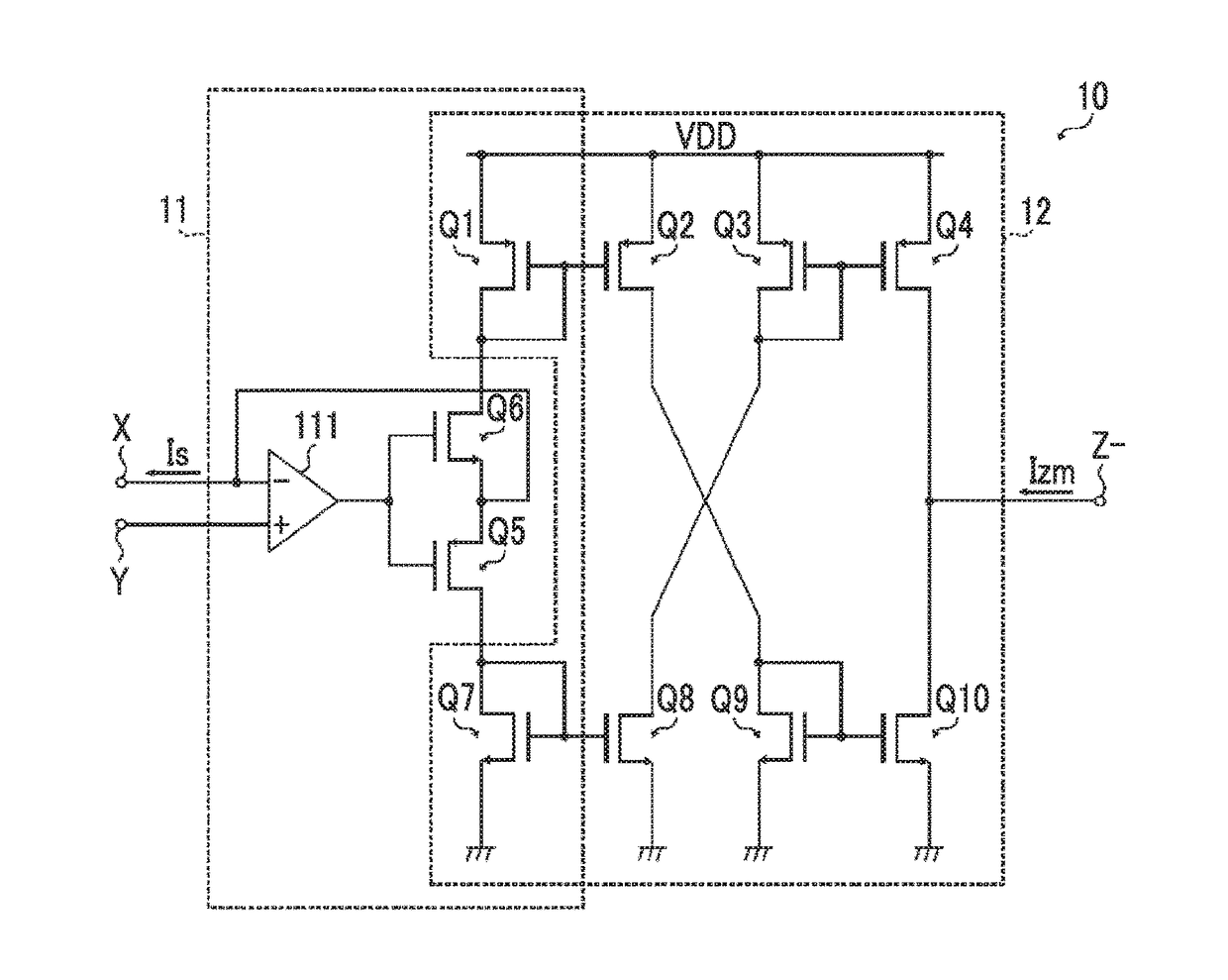
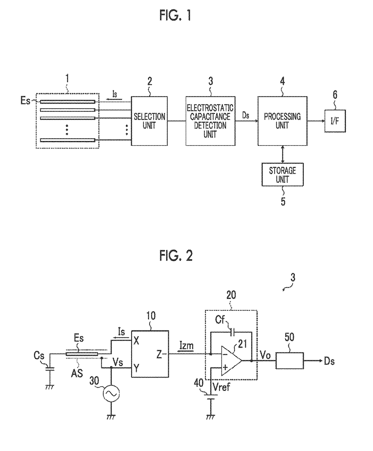
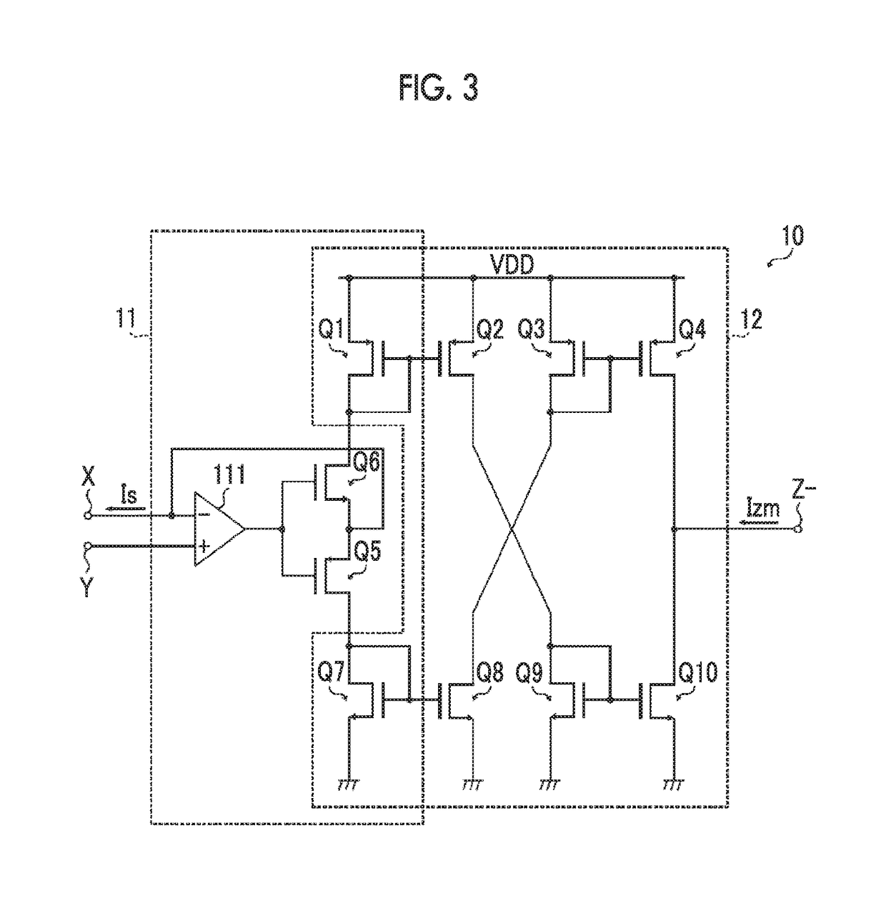
[0043]FIG. 1 is a diagram showing an example of the configuration of an input device according to this embodiment. The input device shown in FIG. 1 has an electrode unit 1, a selection unit 2, an electrostatic capacitance detection unit 3, a processing unit 4, a storage unit 5, and an interface unit 6.

[0044]If an object, such as a finger or a pen, is proximate to a detection electrode in the electrode unit 1, a capacitor formed between the detection electrode Es and the ground changes. The input device according to this embodiment detects and acquires, as information according to the proximity of the object, an electrostatic capacitance value of the capacitor formed between the detection electrode (Es) and the ground. For example, this embodiment is applied to a user interface device (touch pad, touch panel, or the like) which acquires information, such as the presence or absence of proximity of the object to the electrode unit 1, the proximity position of the object, the distance b...

second embodiment

[0093]Next, a second embodiment of the invention will be described. FIG. 7 is a diagram showing a configuration example of a main part of an input device according to the second embodiment. The overall configuration of the input device is the same as that of FIG. 1.

[0094]An electrostatic capacitance detection unit 3 shown in FIG. 7 has a detection current correction circuit 70, in addition to the same configuration as the electrostatic capacitance detection unit 3 shown in FIG. 2. The detection current correction circuit 70 is a circuit which corrects an error due to a parasitic capacitor provided in parallel with the detection-target capacitor Cs. The detection current correction circuit 70 includes a node N1 which is connected to a current path where the detection current Izm flows from the current output circuit 10 to the current-voltage conversion circuit 20, and outputs a correction current Icp for decreasing the amplitude of the detection current Izm from the node N1.

[0095]In ...

third embodiment

[0102]Next, a third embodiment of the invention will be described. FIG. 11 is a diagram showing a configuration example of a main part of an input device according to the third embodiment. The overall configuration of the input device is the same as that of FIG. 1.

[0103]An electrostatic capacitance detection unit 3 shown in FIG. 11 has a configuration in which the detection current correction circuit 70 in the electrostatic capacitance detection unit 3 shown in FIG. 7 is replaced with a detection current correction circuit 70A. The detection current correction circuit 70A has a correction capacitor Ccp, a correction current output circuit 72, and a voltage generation circuit 71.

[0104]The correction current output circuit 72 outputs a current Ix to the correction capacitor Ccp such that a voltage substantially equal to the correction voltage Vcp supplied from the voltage generation circuit 72 is generated in the correction capacitor Ccp, and outputs a correction current Icp proportio...


PUM


Abstract

In a case where the amplitude of a detection voltage is increased, the amplitude of a drive current flowing in a detection-target capacitor also increases, and thus, the amplitude of a detection current also increases. In this case, the increase in amplitude of the detection current is not directly restricted by the condition of a power supply voltage range enabling a circuit to operate. For this reason, a current conversion ratio of a current output circuit or a capacitance value of a capacitor of a current-voltage conversion circuit is set to an appropriate value so as not to cause a voltage to exceed the power supply voltage range, thereby preventing the amplitude of the detection current from being restricted by the condition of the power supply voltage range. Therefore, it is possible to increase the amplitude of the detection voltage to a maximum within the power supply voltage range.

Description

CLAIM OF PRIORITY[0001]This application is a Continuation of International Application No. PCT / JP2015 / 077490 filed on Sep. 29, 2015, which claims benefit of Japanese Patent Application No. 2014-210465 filed on Oct. 15, 2014. The entire contents of each application noted above are hereby incorporated by reference.BACKGROUND OF THE INVENTION[0002]1. Field of the Invention[0003]The present invention relates to an input device which inputs information according to proximity of an object, and for example, to an input device, such as a touch pad or a touch sensor, including detection electrodes whose electrostatic capacitance changes according to proximity of an object.[0004]2. Description of the Related Art[0005]As a user interface device of an information apparatus, such as a smartphone, devices, such as a touch pad and a touch panel, including a sensor configured to detect a touch position of a finger or a pen become widespread. While there are various types, such as a resistive film t...

Claims


Application Information

Patent Timeline
IPC IPC(8): G06F3/044H03K17/955
CPCG06F3/044H03K17/955H03K2017/9455G06F2203/04107G06F2203/04101G06F3/0416G06F3/04182H03K2217/960705
Inventor FUJIYOSHI, TATSUMIHIRATATE, YASUHIKO
Owner ALPS ALPINE CO LTD
Why Eureka
Try Eureka