
OLED display element and its fabricating method, display panel and display device

a technology fabricating methods, applied in the field of display techniques, can solve the problems of reducing the lifetime of oled display elements, and achieve the effects of high fineness, small size and high fineness

Active Publication Date: 2017-07-20
BOE TECH GRP CO LTD +1
View PDF0 Cites 0 Cited by
  • Summary
  • Abstract
  • Description
  • Claims
  • Application Information

AI Technical Summary

Benefits of technology

The disclosure provides a way to improve the resolution and fineness of OLED display elements and panels. This can improve the overall quality of the display and make it easier to display high-quality content.

Problems solved by technology

The presence of water and moisture would decrease the lifetime of the OLED display element.

Method used


Image

  • OLED display element and its fabricating method, display panel and display device
  • OLED display element and its fabricating method, display panel and display device
  • OLED display element and its fabricating method, display panel and display device

Examples


Embodiment Construction

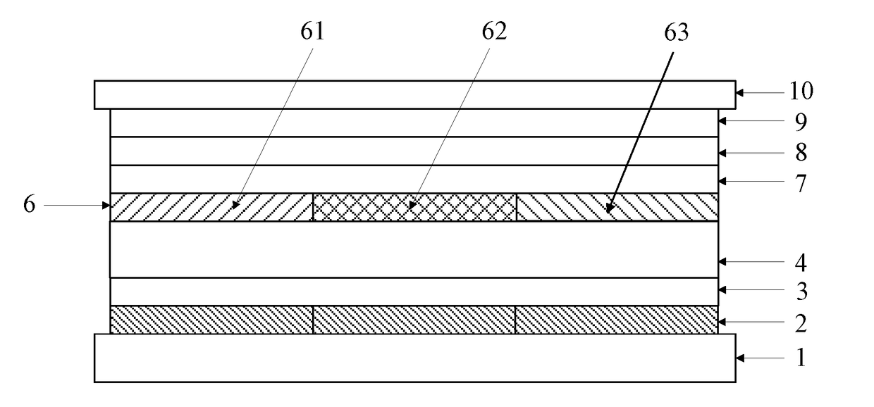
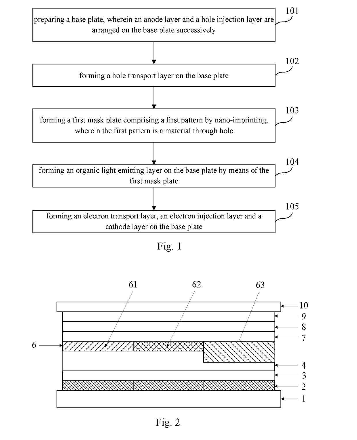
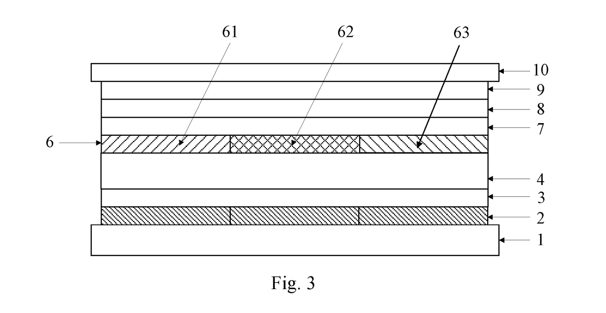
[0029]The specific embodiments of this disclosure shall be explained in details as follows with reference to the drawings. The drawings of this disclosure schematically illustrate structures, portions and / or steps related to the inventive concepts, but do not illustrate or only partially illustrate structures, portions and / or steps unrelated to the inventive concepts. However, a more fine FMM is currently not available. Therefore, the AMOLED display element fabricated by the FMM technology has a low fineness, so that the display panel comprising the AMOLED display element fabricated by the FMM technology has a low resolution. Thus, there is a need for improving the resolution of the display panel in the art.

[0030]As shown in FIG. 1, in an embodiment of the present disclosure, a method for fabricating an OLED display element is disclosed. The OLED display element corresponds to a pixel unit. The method comprises the following steps. 101, preparing a base plate, wherein an anode layer...


PUM

PropertyMeasurementUnit
temperatureaaaaaaaaaa
currentaaaaaaaaaa
brightnessaaaaaaaaaa

Abstract

An OLED display element and its fabricating method, a display panel and a display device are disclosed. The method comprises steps of: preparing a base plate, wherein an anode layer and a hole injection layer are arranged on the base plate successively; forming a hole transport layer on the base plate; forming a first mask plate comprising a first pattern by nano-imprinting, wherein the first pattern is a material through hole; forming an organic light emitting layer on the base plate by means of the first mask plate; and forming an electron transport layer, an electron injection layer and a cathode layer on the base plate. The fabricated OLED display element has a relatively small size and relatively high fineness. Thus, in case the OLED display element is applied to a display panel, the resolution of the display panel is increased.

Description

RELATED APPLICATIONS[0001]The present application is the U.S. national phase entry of PCT / CN2015 / 090907, with an international filing date of Sep. 28, 2015, which claims the benefit of Chinese Patent Application No. 201510354557.X, filed on Jun. 24, 2015, the entire disclosures of which are incorporated herein by reference.FIELD OF THE INVENTION[0002]The present disclosure relates to the field of display technique, and in particular to an OLED display element and its fabricating method, a display panel and a display device.BACKGROUND ART[0003]An OLED (Organic Light Emitting Diode) display element is a device in which organic semiconductor films are activated to emit light by a current. The OLED display element has a sandwich structure, and generally comprises an anode, a hole injection layer, a hole transport layer, an organic light emitting layer, an electron transport layer and a cathode. Under the effect of an external electric field, electrons and holes are respectively injected...

Claims


Application Information

Patent Timeline
Patent Type & Authority Applications(United States)
IPC IPC(8): H01L51/56H01L51/00H01L27/32H01L51/50H10K99/00
CPCH01L51/56H01L51/5056H01L51/5072H01L51/5092H01L2227/323H01L51/0004H01L27/3244H01L27/3211H01L51/0026H01L51/5096H10K50/15H10K50/11H10K50/181H10K71/13H10K71/20H10K71/00H10K50/16H10K50/18H10K50/171H10K59/12H10K59/35H10K71/40H10K59/1201
Inventor YANG, JIUXIABAI, FENG
Owner BOE TECH GRP CO LTD
Learn More