This helps you quickly interpret patents by identifying the three key elements:
Problems solved by technology
Method used
Benefits of technology
Benefits of technology
The disclosed fabrication method for wafer-level packaging has advantages over existing technologies. By using a certain order and method, the thickness of the chip stack is reduced, and a flip packaging of the chip is achieved without destroying the chip structure. This reduces the processing risks and improves the overall efficiency of the packaging process.
Problems solved by technology
However, processing risks may be increased accordingly.
Method used
Image
Click on the blue label to locate the original text in one second.
Reading with bidirectional positioning of images and text.
Examples
first embodiment
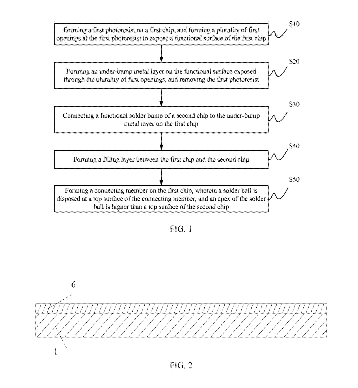
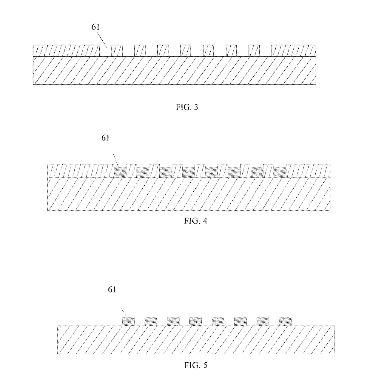
[0032]First, as shown in FIG. 2, a first photoresist 6 may be formed on a first chip 1. As shown in FIG. 3, a plurality of first openings 61 may be formed on the first photoresist to expose a functional surface of the first chip.
[0033]Next, as shown in FIG. 4, an under-bump metal layer 11 may be formed on the functional surface exposed by the plurality of first openings 61. Then the first photoresist may be removed, and the corresponding structure is shown in FIG. 5.
[0034]Next, a plurality of functional solder bumps of a second chip 2 may be connected to the under-bump metal layer of the first chip.
[0035]Next, a filling layer 5 may be disposed between the first chip and the second chip, and the corresponding structure is shown in FIG. 7
[0036]Finally, a connecting member is formed on the first chip. A solder ball may be disposed on the top surface of the connecting member, and the apex of the solder ball is higher than the top surface of the second chip.
[0037]Further, as shown in FIG...
second embodiment
[0047]Referring to FIGS. 2-8, the first chip and the second chip may be disposed face-to-face, and the filling layer 5 may be formed between the first chip 1 and the second chip 2. After the filling layer 5 is formed between the first chip 1 and the second chip 2, a vapor deposition layer (not shown in the drawings) may be formed on an entire structure including the first chip, the second chip, and the filling layer. Then the second photoresist 7 may be formed on the vapor deposition layer, as FIG. 8 shows. These abovementioned steps are the same as the corresponding steps disclosed by the first embodiment.
[0048]As shown in FIG. 13, then a plurality of second openings 71′ may be formed on the second photoresist 7 to expose the vapor deposition layer, through which a portion of the vapor deposition layer may be exposed. A connecting base may be formed on the exposed vapor deposition layer. Then the second photoresist may be removed to expose the remained vapor deposition layer, and a...
third embodiment
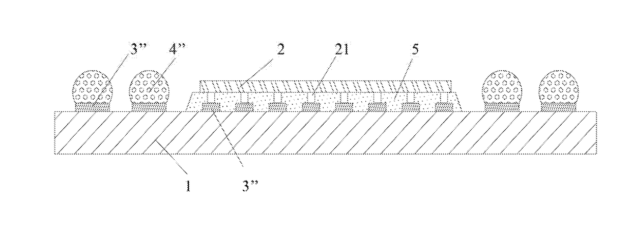
[0056]First, as shown in FIG. 2, the first photoresist 6 may be formed on the first chip 1, which is similar to the above-disclosed embodiments. As shown in FIG. 17, a plurality of first openings 61′ may be formed on the first photoresist 6, and the first openings 61′ in FIG. 17 may be formed in a similar way as the first openings 61 in FIG. 3. However, the number of the first openings 61′ in FIG. 17 may be significantly larger than the number of the first openings 61 in FIG. 3, such that when the under-bump metal layer subsequently formed on the first chip is connected to the functional solder bump of the second chip, the under-bump metal layer may be partially vacated.
[0057]Next, as shown in FIG. 18, an under-bump metal layer 3″ may be formed on the functional surface exposed by the plurality of first openings 61″. Then the first photoresist may be removed, and the corresponding structure is shown in FIG. 19. The under-bump metal layer 3″ may be formed on the first chip.
[0058]Next...
PUM
Abstract
The present disclosure discloses a fabrication method for wafer-level packaging, comprising: forming a first photoresist on a first chip and a plurality of first openings at the first photoresist to expose a functional surface of the first chip, forming an under-bump metal layer on the functional surface exposed through the plurality of first openings, and removing the first photoresist; connecting a functional solder bump of a second chip to the under-bump metal layer on the first chip; forming a filling layer between the first chip and the second chip; and forming a connecting member on the first chip, wherein a solder ball is disposed at a top surface of the connecting member, and an apex of the solder ball is higher than a top surface of the second chip. The first chip and the second chip are disposed face-to-face, and the filling layer is formed between the first chip and the second chip. The solder ball is mounted on the connecting member. A certain height difference is formed between the solder ball and the second chip, such that a flip packaging of the chip is realized while the chip is not destroyed. The second chip will not be destroyed during the flip packaging, thereby reducing the processing risks.
Description
FIELD OF THE DISCLOSURE[0001]The present disclosure relates to semiconductor fabrication methods, and more specifically, relates to a fabrication method for wafer-level packaging.BACKGROUND[0002]Since chips have more and more functions, the requirements for chip packaging become higher and higher. Flip packaging and stack packaging of chips have become a trend and, meanwhile, the packaging thickness is desired to be as thin as possible, which to a certain degree requires the chip packaging to be as thin as possible. However, processing risks may be increased accordingly.BRIEF SUMMARY OF THE DISCLOSURE[0003]In the following, an overview of the present disclosure is given simply to provide basic understanding to some aspects of the present disclosure. It should be understood that this overview is not an exhaustive overview of the present disclosure. It is not intended to determine a critical part or an important part of the present disclosure, nor to limit the scope of the present dis...
Claims
Application Information
Patent Timeline
Application Date:The date an application was filed.
Publication Date:The date a patent or application was officially published.
First Publication Date:The earliest publication date of a patent with the same application number.
Issue Date:Publication date of the patent grant document.
PCT Entry Date:The Entry date of PCT National Phase.
Estimated Expiry Date:The statutory expiry date of a patent right according to the Patent Law, and it is the longest term of protection that the patent right can achieve without the termination of the patent right due to other reasons(Term extension factor has been taken into account ).
Invalid Date:Actual expiry date is based on effective date or publication date of legal transaction data of invalid patent.

