Array substrate and preparation method thereof and display panel

An array substrate and substrate layer technology, which is applied to instruments, semiconductor devices, electrical components, etc., can solve the problems of incompatibility between design and manufacturing process, damage to the electrical properties of the IGZO layer, and different etching of deep and shallow holes, so as to save manufacturing costs and save The overall process steps, the effect of optimizing the process

Inactive Publication Date: 2020-02-21
WUHAN CHINA STAR OPTOELECTRONICS TECH CO LTD
View PDF7 Cites 2 Cited by
  • Summary
  • Abstract
  • Description
  • Claims
  • Application Information

AI Technical Summary

Problems solved by technology

[0005] However, for the LTPO array substrate, there are many design and process incompatibility problems between the LTPS TFT and Oxide TFT disposed on it at the same time.
For example, the Pre-Clean (HF solution) solution used in the SD process in LTPS TFT will etch the IGZO layer in Oxide TFT, and the ILD layer in LTPS TFT will contain a large amount of residual H after it is completed, which will destroy the IGZO layer in Oxide TFT. The electrical properties of the IGZO layer, and the film thickness requirements of the shared film layer of LTPS TFT and Oxide TFT are inconsistent, and the etching of deep and shallow holes is different due to the different thickness of the two, etc.

Method used


Image

  • Array substrate and preparation method thereof and display panel
  • Array substrate and preparation method thereof and display panel
  • Array substrate and preparation method thereof and display panel

Examples


Embodiment Construction

[0044] A TFT array substrate, a manufacturing method thereof and a technical solution of a display panel of the present invention will be further described in detail with reference to the accompanying drawings and embodiments.

[0045] Wherein, since the present invention also relates to a TFT array substrate and its preparation method, in order to avoid unnecessary repetition, the structure of the TFT array substrate involved in the present invention will be described below in conjunction with the preparation method of the TFT array substrate involved in the present invention. Illustrate by example.

[0046] One embodiment of the present invention provides a method for preparing a TFT array substrate, which includes the following steps:

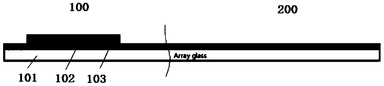
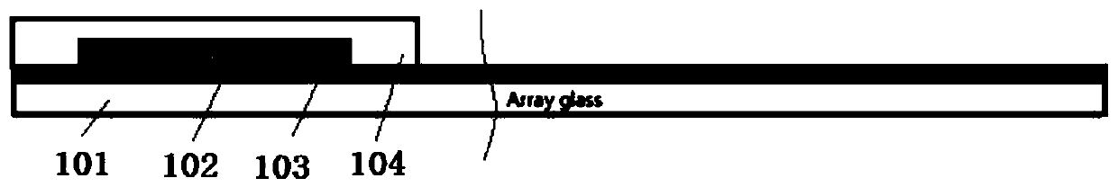
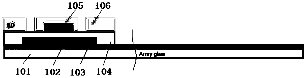
[0047] Step S1 , providing a substrate layer, which defines a first region 100 and a second region 200 , and the first TFT is fabricated in the first region of the substrate layer. Wherein the first area 100 is preferably a GOA area, and th...


PUM


Abstract

The invention provides a TFT array substrate and a preparation method thereof and a display panel. The TFT array substrate is defined with a first area and a second area, a first TFT is arranged on the first area, and a second TFT is arranged on the second area. The first TFT is a top gate type TFT, the second TFT is a bottom gate type TFT, and the material adopted by a source-drain layer of the first TFT is consistent with the material adopted by a gate layer of the second TFT. The TFT array substrate provided by the invention is designed by adopting a novel film layer structure, so that thefirst TFT and the second TFT arranged on the TFT array substrate can be well compatible in design and manufacturing process, and the manufacturing process risk of the array substrate where the first TFT and the second TFT are located is reduced.

Description

technical field [0001] The present invention relates to the technical field of flat display, in particular, an array substrate, a preparation method thereof and a display panel thereof. Background technique [0002] It is known that with the continuous development of display technology, new flat panel displays have begun to completely replace CRT displays and become mainstream display devices in the market. [0003] Among them, Liquid Crystal Display (LCD) is widely used in mobile phones, TVs, personal digital assistants, and digital cameras due to its own advantages such as high image quality, power saving, thin body, and wide application range. , Notebook computers, desktop computers and other consumer electronics products have become the mainstream of display devices. [0004] In recent years, LCD devices have shown a development trend of high resolution, narrow frame and low power consumption. In order to find a more power-saving solution with limited space and battery...

Claims


Application Information

Patent Timeline
Patent Type & Authority Applications(China)
IPC IPC(8): H01L27/12G02F1/1333
CPCH01L27/1214H01L27/1251H01L27/1259G02F1/1333G02F1/13624H01L27/1225G02F1/134363G02F1/13454G02F1/1368H01L27/1288
Inventor 肖军城艾飞尹国恒许勇
Owner WUHAN CHINA STAR OPTOELECTRONICS TECH CO LTD
Why Eureka
Try Eureka