Display device and method for manufacturing the same

a technology of a display device and a manufacturing method, applied in the field of display devices, can solve the problems of short circuit of neighboring pixel electrodes, and achieve the effect of high precision

Active Publication Date: 2017-08-03
JAPAN DISPLAY INC
View PDF1 Cites 6 Cited by
  • Summary
  • Abstract
  • Description
  • Claims
  • Application Information

AI Technical Summary

Benefits of technology

[0010]The present invention is directed to enabling a formation of the pixel electrode that can be hardly peeled off and patterning thereof with a high precision.

Problems solved by technology

Therefore, there is a problem that neighboring pixel electrodes are short-circuited since the patterning by the mixed acid is not enough.

Method used


Image

  • Display device and method for manufacturing the same
  • Display device and method for manufacturing the same
  • Display device and method for manufacturing the same

Examples


first embodiment

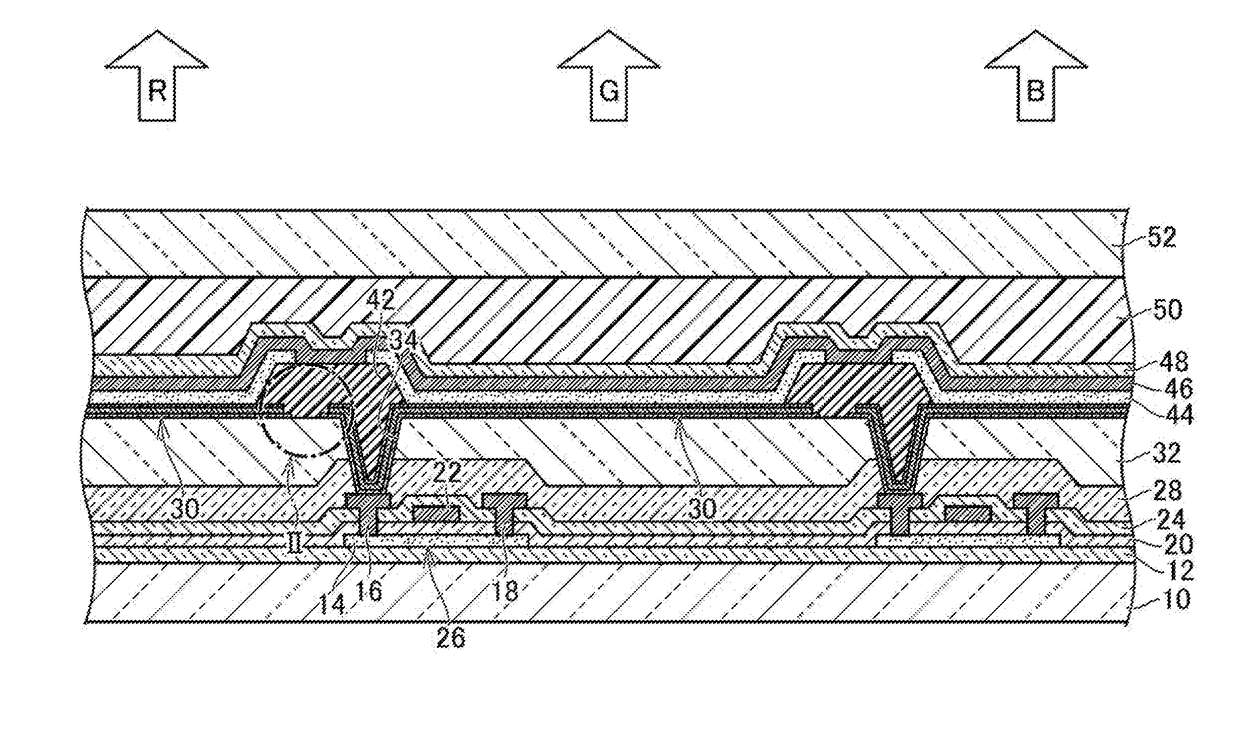
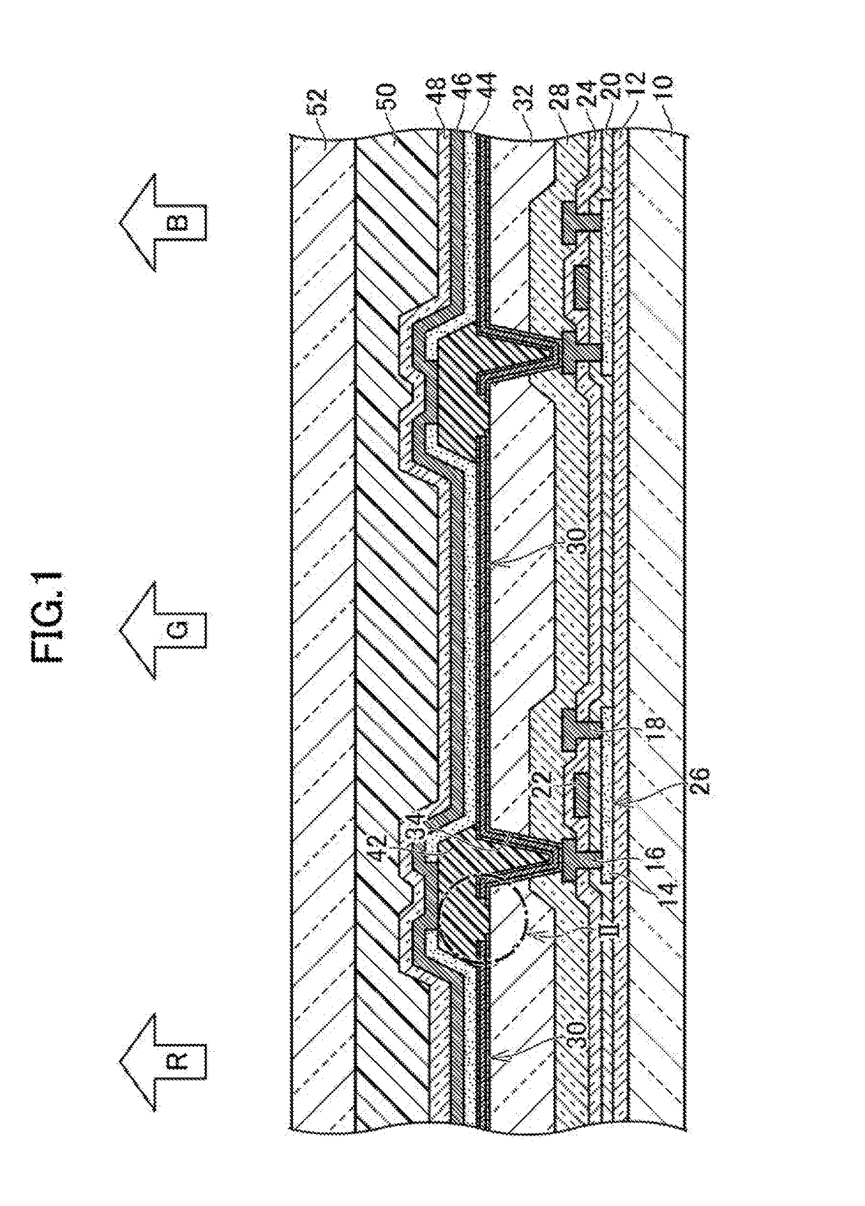
[0031]FIG. 1 is a cross sectional view of a display device according to a first embodiment of the present invention. As a display device, an organic electroluminescence display device is mentioned as an example. The display device is configured to combine unit pixels of a plurality of colors composed of, for example, red (R), green (G) and blue (B) (subpixels) to form a pixel of full color (a pixel) and display an image of full color.

[0032]The display device includes a first substrate 10 made of glass or resin. On the first substrate 10, an undercoat 12 that becomes a barrier to prevent impurities that are contained in the first substrate 10 itself from spreading toward upper layers is formed, and a semiconductor layer 14 is formed thereon. A source electrode 16 and a drain electrode 18 are provided on the semiconductor layer 14, and a gate insulating film 20 is formed covering the semiconductor layer 14. On the gate insulating film 20, a gate electrode 22 is formed, and an interlay...

second embodiment

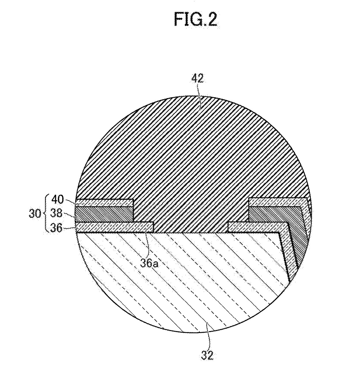
[0053]FIG. 5 is a magnified cross sectional view illustrating a part of a display device according to a second embodiment of the present invention. In this embodiment, a pixel electrode 230 is formed on a base layer 232, and an inorganic insulating layer 262 is put on at least a tip of a protrusion part 236a of the first oxide conductive layer 236 and on the base layer 232. The inorganic insulating layer 262 is formed with a space from a tip of a metal conductive layer 238 and a tip of a second oxide conductive layer 240. That is, the inorganic insulating layer 262 is provided separately from the base layer 232.

[0054]FIGS. 6A to 7B are views illustrating a manufacturing method of the display device according to the second embodiment of the present invention.

[0055]As illustrated in FIG. 6A, a pattern of the first oxide conductive layer 236 is formed on the base layer 232, and further the inorganic insulating layer 262 made of silicon nitride, silicon dioxide, or the like is formed. A...


PUM

PropertyMeasurementUnit
conductiveaaaaaaaaaa
adhesionaaaaaaaaaa
light extraction efficiencyaaaaaaaaaa

Abstract

A display device includes: a base layer; pixel electrodes laminated on the base layer; a light emitting element layer laminated on the pixel electrodes; and a common electrode laminated on the light emitting element layer. Each of the pixel electrodes includes a first oxide conductive layer that is in direct contact with the base layer, a metal conductive layer that is in direct contact with the first oxide conductive layer, and a second oxide conductive layer that is in direct contact with the metal conductive layer. The base layer has an adhesion to the first oxide conductive layer that is higher than that of the metal conductive layer. The first oxide conductive layer includes a protrusion part that is extended farther than the metal conductive layer and the second oxide conductive layer in a direction, adjacent two of the pixel electrodes facing each other in the direction.

Description

CROSS-REFERENCE TO RELATED APPLICATION[0001]The present application claims priority from Japanese application JP2016-018153 filed on Feb. 2, 2016, the content of which is hereby incorporated by reference into this application.BACKGROUND OF THE INVENTION[0002]1. Field of the Invention[0003]The present invention relates to a display device and a manufacturing method thereof.[0004]2. Description of the Related Art[0005]A display device on which a light emitting element such as an organic electroluminescent element is provided for each pixel is expected to be a display of the next generation. A light emitting element is configured to emit light in a light emitting layer held between a pixel electrode (anode) and a common electrode (anode), the common configuration is to reflect the emitted light at the pixel electrode. In the case of a display device of the top emission type, since emitted light from the light emitting element is extracted from the common electrode side, the pixel elect...

Claims


Application Information

Patent Timeline
Patent Type & Authority Applications(United States)
IPC IPC(8): H01L27/12H01L27/32
CPCH01L27/124H01L27/3276H01L2227/323H01L27/3258H01L27/1259H01L27/1248H10K59/123H10K59/131H10K71/00H10K59/124H10K50/818H10K2102/341H10K50/81H10K50/813H10K59/1201
Inventor KANDA, NORIYOSHI
Owner JAPAN DISPLAY INC
Why Eureka
Try Eureka