Semiconductor package and method of manufacturing semiconductor package

a technology of semiconductor packaging and semiconductor components, applied in the direction of semiconductor devices, semiconductor/solid-state device details, electrical devices, etc., can solve the problems of preventing the reduction of the size and thickness of portable wireless communication devices such as smart phones,

Active Publication Date: 2017-08-17
DISCO CORP
View PDF6 Cites 4 Cited by
  • Summary
  • Abstract
  • Description
  • Claims
  • Application Information

AI Technical Summary

Benefits of technology

[0006]Therefore, it is an object of the present invention to provide a semiconductor package which is capable of blocking electromagnetic noise that tends to have an adverse effect on a wireless system, without employing a sheet metal shield, and a method of manufacturing such a semiconductor package.
[0009]According to the present invention, the electromagnetic wave shield film is formed on the upper surface of the layer of sealing resin on each of the semiconductor packages and the side surfaces of each of the semiconductor packages. Each of the semiconductor packages is of such a structure that when it is mounted on a mother substrate, the electromagnetic wave shield film is grounded, i.e., connected to a ground pattern on the mother substrate. Therefore, each semiconductor package does not have an adverse effect on a wireless system in a wireless communication device which incorporates the semiconductor package therein, even though no sheet metal shield is employed in the semiconductor package.

Problems solved by technology

However, the sheet metal shield disclosed in Japanese Patent Laid-Open Nos. 2001-44680 and 2004-72051 needs a large area where it is to be installed, and hence presents an obstacle to efforts to reduce the size and thickness of portable wireless communication devices such as mobile phones, smart phones, etc.

Method used


Image

  • Semiconductor package and method of manufacturing semiconductor package
  • Semiconductor package and method of manufacturing semiconductor package
  • Semiconductor package and method of manufacturing semiconductor package

Examples


Embodiment Construction

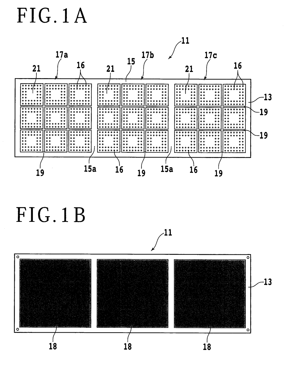
[0022]Preferred embodiments of the present invention will be described in detail below with reference to the drawings. FIG. 1A depicts in plan a package substrate 11 including semiconductor packages in the form of ball grid array (BGA) packages according to a first embodiment of the present invention. FIG. 1B depicts the reverse side of the package substrate 11. The package substrate 11 has a rectangular resin substrate 13 including an outer peripheral extra region 15 and non-device regions 15a which jointly surround a plurality of (three in the illustrated embodiment) device regions 17a, 17b and 17c. According to the present embodiment, the substrate 13 is made of resin. However, the resin substrate 13 may be replaced with a silicon substrate.

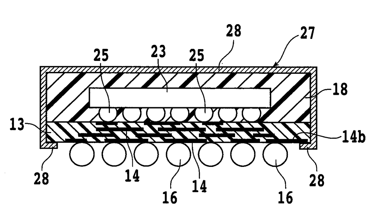
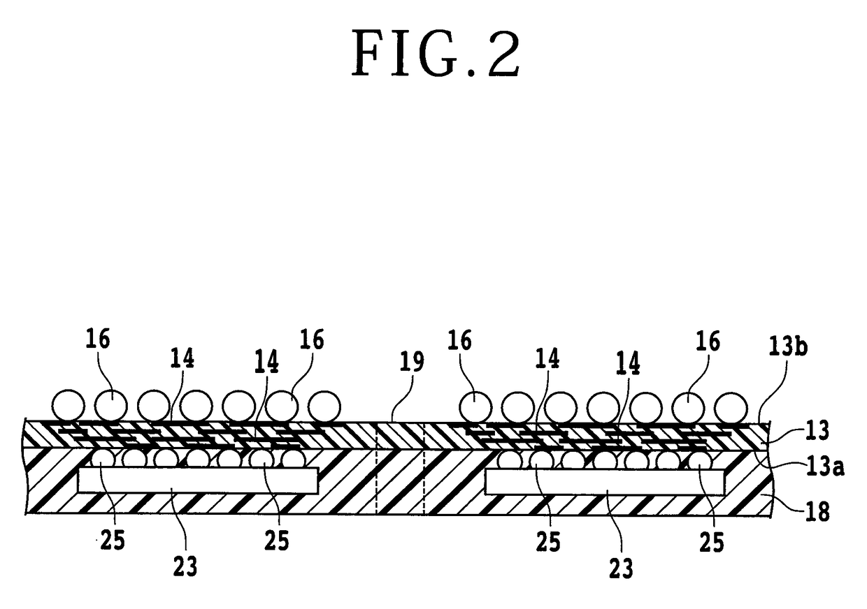
[0023]Each of the device regions 17a, 17b and 17c is demarcated into a matrix of device placement areas 21 by a plurality of projected dicing lines 19 which extend perpendicularly to each other. As depicted in FIG. 2, a semiconductor device 23...


PUM


Abstract

A semiconductor package includes a substrate having a first surface, a second surface opposite the first surface, and interconnect patterns disposed therein, a semiconductor device mounted on the first surface of the substrate, a layer of sealing resin sealing the semiconductor device, a plurality of external connection electrodes formed on the second surface of the substrate, an electromagnetic wave shield film for blocking electromagnetic waves, which is formed on an upper surface of the layer of sealing resin and side surfaces of the layer of sealing resin and the substrate, and a ground interconnect formed on the substrate and electrically connected to the electromagnetic wave shield film.

Description

BACKGROUND OF THE INVENTION[0001]Field of the Invention[0002]The present invention relates to a semiconductor package and a method of manufacturing a semiconductor package.[0003]Description of the Related Art[0004]In recent years, portable wireless communication devices such as mobile phones, smart phones, etc. have been incorporating an increased number of electronic parts including a surface acoustic wave (SAW) device, an antenna element, etc. that make up a wireless system installed therein in order to give themselves high functionality and high performance. Various semiconductor packages such as dynamic random access memories (DRAMs), flash memories, etc. for use in such portable wireless communication devices have data transfer rates that have become so high that electromagnetic waves generated by the semiconductor packages are liable to act as noise that has an adverse effect on the wireless system in the portable wireless communication devices. One solution to this problem is...

Claims


Application Information

Patent Timeline
Patent Type & Authority Applications(United States)
IPC IPC(8): H01L23/552H01L23/498H01L21/78H01L21/48H01L21/56H01L23/00H01L23/31
CPCH01L23/552H01L24/16H01L23/49822H01L23/49838H01L23/49811H01L23/3114H01L2924/3025H01L21/4853H01L21/4857H01L21/565H01L21/78H01L2224/16227H01L21/485H01L23/3128H01L21/561H01L24/97H01L2224/97H01L2924/15311H01L23/145H01L23/147H01L23/49827H01L21/4867H01L21/6836H01L2221/68331H01L2224/81H01L23/60H01L23/62H01L21/56
Inventor SUZUKI, KATSUHIKO
Owner DISCO CORP
Why Eureka
Try Eureka