Spin-orbit logic with charge interconnects and magnetoelectric nodes

Active Publication Date: 2017-08-24
INTEL CORP
View PDF3 Cites 32 Cited by
  • Summary
  • Abstract
  • Description
  • Claims
  • Application Information

AI Technical Summary

Problems solved by technology

Existing spintronic logic options generally suffer from high energy and relatively long switching timers due to the inefficiency of mechanisms for converting charge to spin variables and vice versa.
In particular, this res

Method used


Image

  • Spin-orbit logic with charge interconnects and magnetoelectric nodes
  • Spin-orbit logic with charge interconnects and magnetoelectric nodes
  • Spin-orbit logic with charge interconnects and magnetoelectric nodes

Examples


example 1

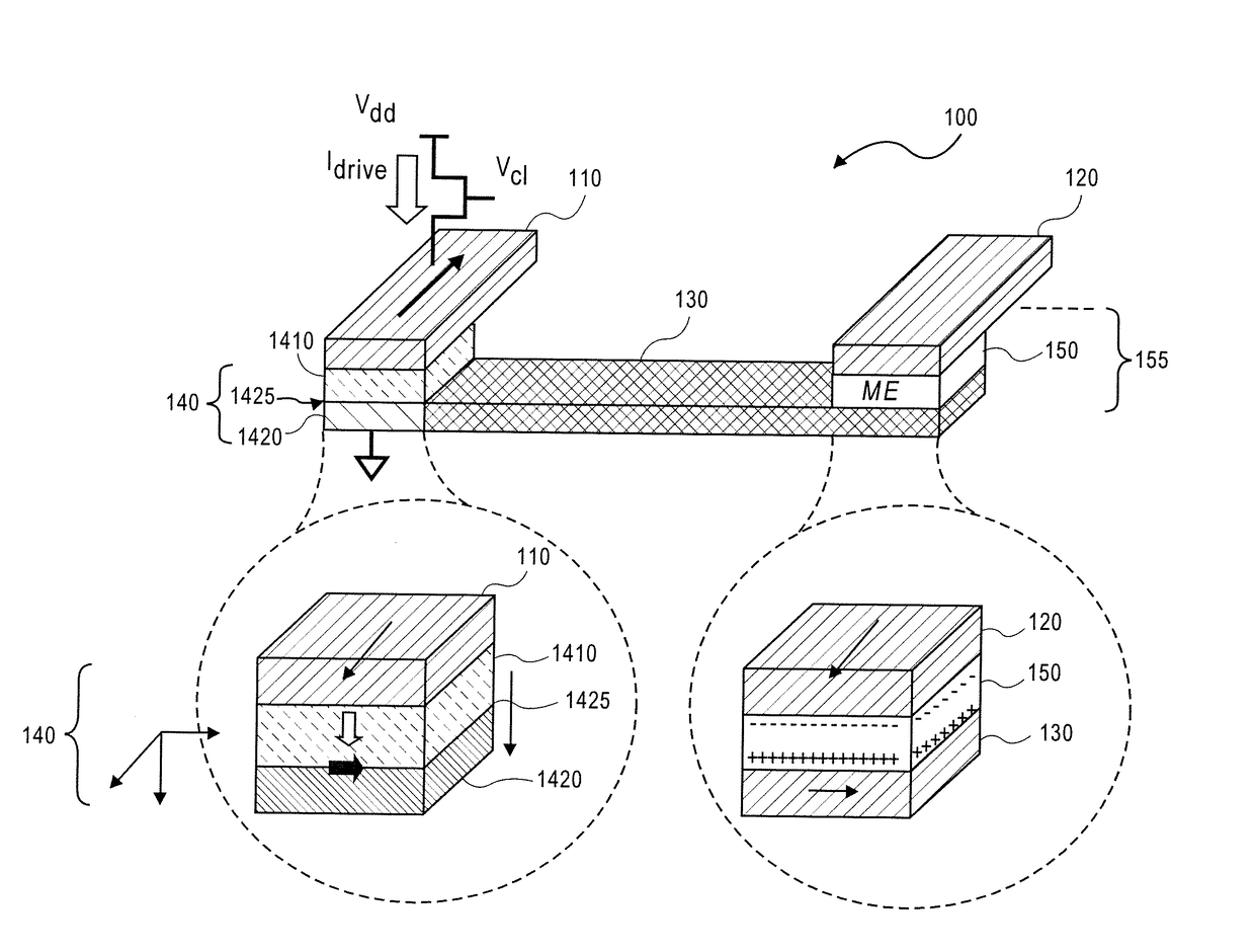
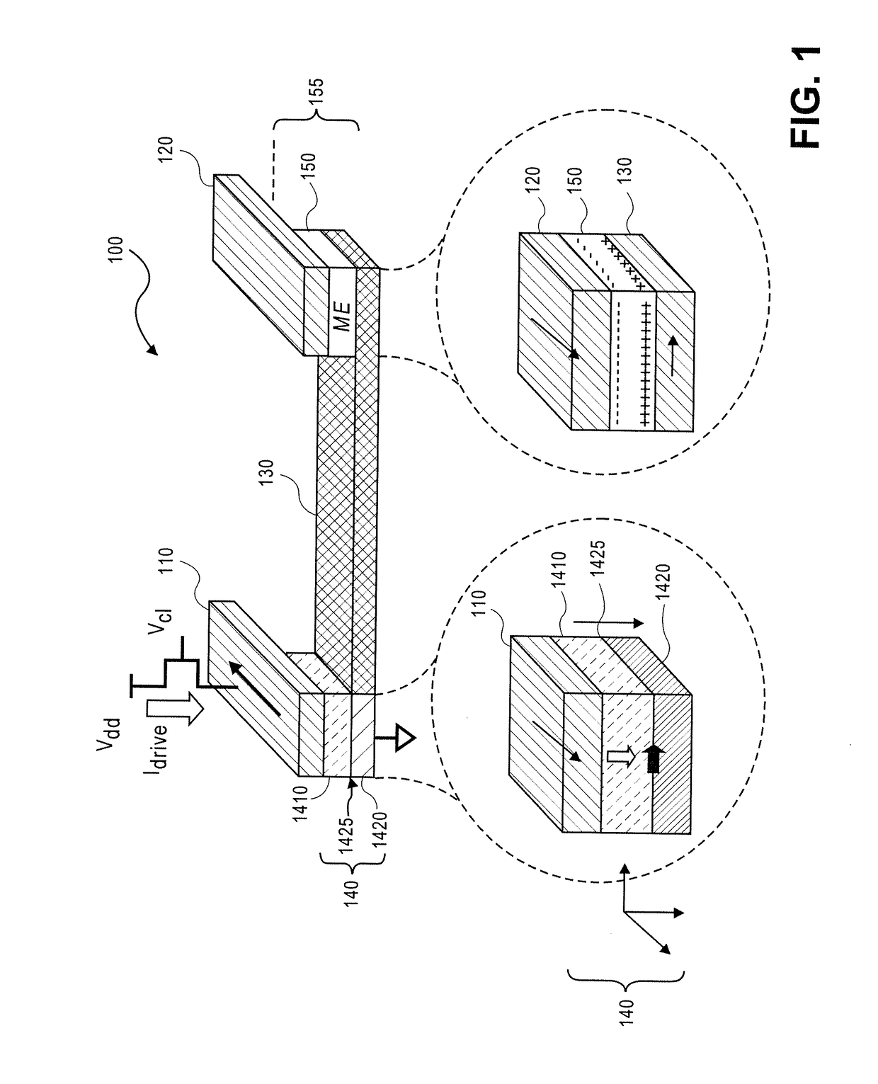
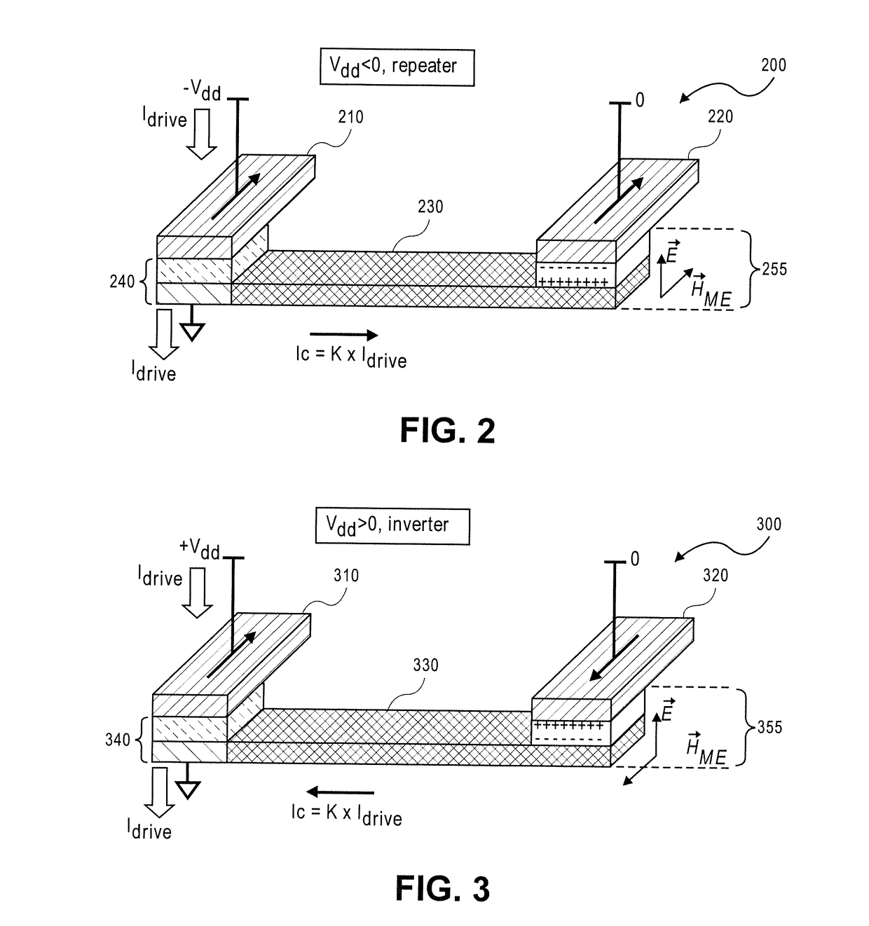
[0058 is an apparatus including a spin to charge conversion node; and a charge to spin conversion node, wherein an input to the spin to charge conversion node produces an output at the charge to spin conversion node.

[0059]In Example 2, the spin to charge conversion node in the apparatus of Example 1 includes a magnet coupled to at least one material, wherein a spin current generated by the magnet is operable to create a transverse charge current in the material.

[0060]In Example 3, the at least one material in the apparatus of Example 2 will exhibit a spin orbit effect in a metallic system.

[0061]In Example 4, the at least one material in the apparatus of Example 3 will produce a spin orbit coupling in response to a spin current.

[0062]In Example 5, the at least one material in the apparatus of Example 3 includes a spin hall effect (SHE) coefficient.

[0063]In Example 6, the at least one material in the apparatus of Example 2 includes a material stack comprising a first material includin...


PUM


Abstract

An apparatus including a spin to charge conversion node; and a charge to spin conversion node, wherein an input to the spin to charge conversion node produces an output at the charge to spin conversion node. An apparatus including a magnet including an input node and output node, the input node including a capacitor operable to generate magnetic response in the magnet and the output node including at least one spin to charge conversion material. A method including injecting a spin current from a first magnet; converting the spin current into a charge current operable to produce a magnetoelectric interaction with a second magnet; and changing a direction of magnetization of the second magnet in response to the magnetoelectric interaction. A method including injecting a spin current from an input node of a magnet; and converting the spin current into a charge current at an output node of the magnet.

Description

BACKGROUND[0001]Field[0002]Integrated circuit devices.[0003]Description of Related Art[0004]Spintronic logic describes a class of integrated circuit devices utilizing a physical variable of magnetization or spin as a computation variable. Such variables can be non-volatile, i.e., preserving a computation state when the power to an integrated circuit is switched off. Non-volatile logic can improve the power and computational efficiency by allowing architects to put a processor to un-powered sleep states more often enabling computation with less energy.[0005]Existing spintronic logic options generally suffer from high energy and relatively long switching timers due to the inefficiency of mechanisms for converting charge to spin variables and vice versa. In particular, this results in large write currents (on the order of 100 microamperes per bit (μA / bit) producing high Joule heat dissipation, and slow switching time (on the order of 10 nanoseconds (ns)) over which the current needs to...

Claims


Application Information

Patent Timeline
IPC IPC(8): H01L27/22H03K19/173H03K19/18
CPCH01L27/22H03K19/173H03K19/18H10B61/00H10N59/00H10N50/00H10B61/22H10N50/80H10N50/10
Inventor MANIPATRUNI, SASIKANTHNIKONOV, DMITRI E.YOUNG, IAN A.
Owner INTEL CORP
Why Eureka
Try Eureka