Method for producing a conductive multiple substrate stack

Active Publication Date: 2017-09-07
EV GRP E THALLNER GMBH
View PDF6 Cites 1 Cited by
  • Summary
  • Abstract
  • Description
  • Claims
  • Application Information

AI Technical Summary

Benefits of technology

[0019]The greatest advantage of the invention includes the fact that it is possible to dispense with (optical) alignment plants, particularly completely, and the substrate stack is able to exploit an extremely wide wavelength spectrum. According to the invention, it is possible to dispense with (optical) alignment plants, because the elements responsible for the conductive connection, particularly TSVs, contacts, passages, holes or nanoparticles permit a tolerance in the position of the substrates with respect to one another. Insofar as contacting plants comprise alignment, that is to say are also understood in the broadest sense as alignment plants, the selection of an alignment plant with a tolerance or alignment accuracy greater than 0.1 μm, preferably greater than 1 μm, more preferably greater than 10 μm, most preferably greater than 100 μm, most preferably of all greater than 1 mm, is sufficient. As a result, the alignment can not only take place substantially faster, rather the alignment plant can be produced in a substantially less expensive manner.
[0020]Furthermore, an embodiment according to the invention advantageously includes the substrate surface comprising a material, particularly an oxide, which is suitable for direct bonding and/or fusion bonding. As a result, the connection of the two substrates to one another is particularly facilitated by the utilization of fusion bonding technology.
[0021]The in

Problems solved by technology

There are diverse technical problems in the production of conductive multiple-substrate stacks, particularly for generating electricity:generating the greatest amount of electricity possible for the lowest possible area,mas

Method used


Image

  • Method for producing a conductive multiple substrate stack
  • Method for producing a conductive multiple substrate stack
  • Method for producing a conductive multiple substrate stack

Examples


Embodiment Construction

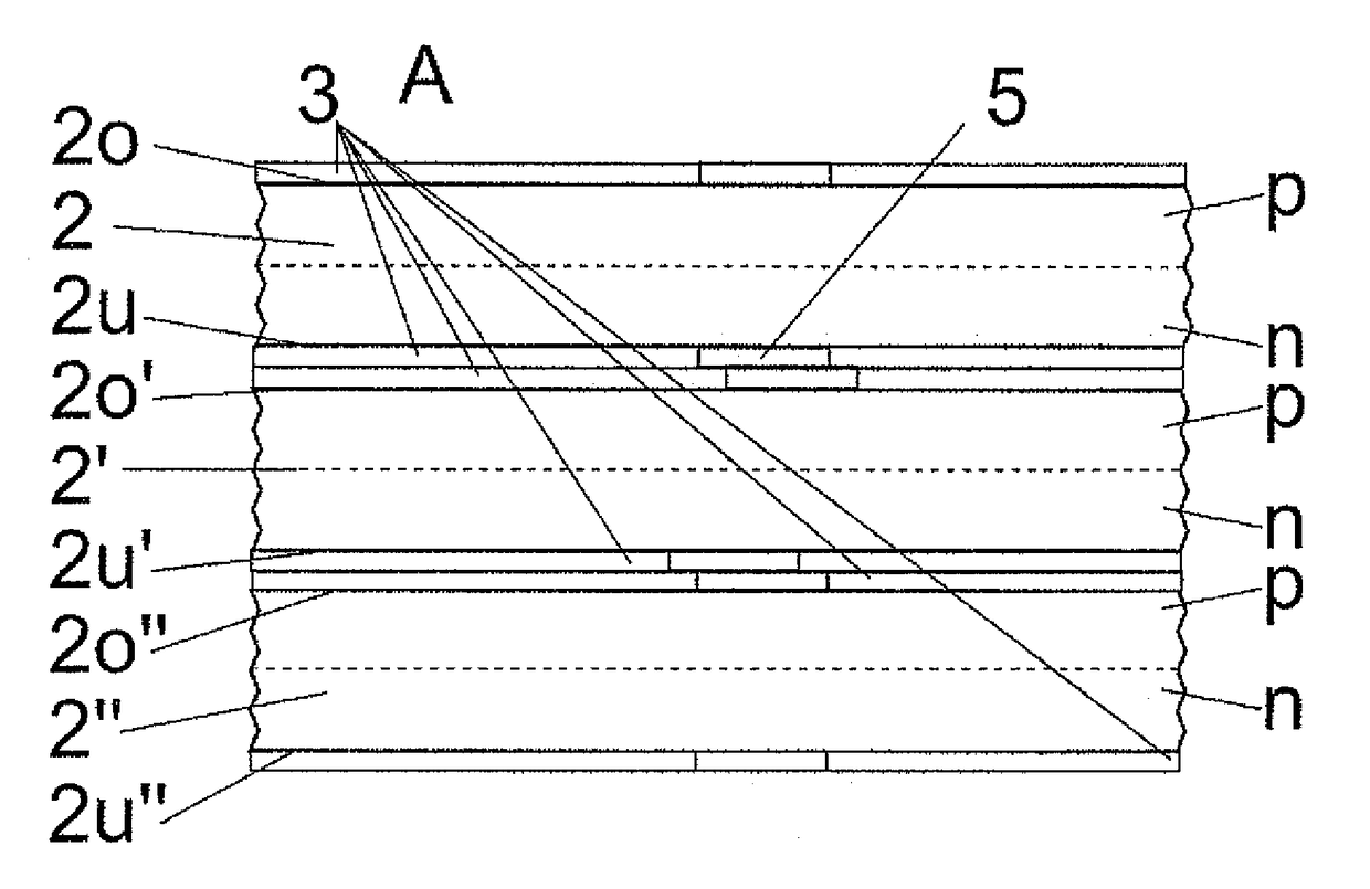
[0098]FIG. 1 shows a schematic cross-sectional view of a substrate stack 1 according to the invention, comprised of three substrates 2, 2′, 2″, The stacking of more or fewer than three substrates 2, 2′, 2″ is also conceivable. The wavelength sensitivity of the substrates is symbolized by wave trains with different wavelength, which represent the electromagnetic waves, in the sense of the partial image, actually the photons. Corresponding contacts for tapping the total voltage generated by the solar cell stack on the outer side are not shown.

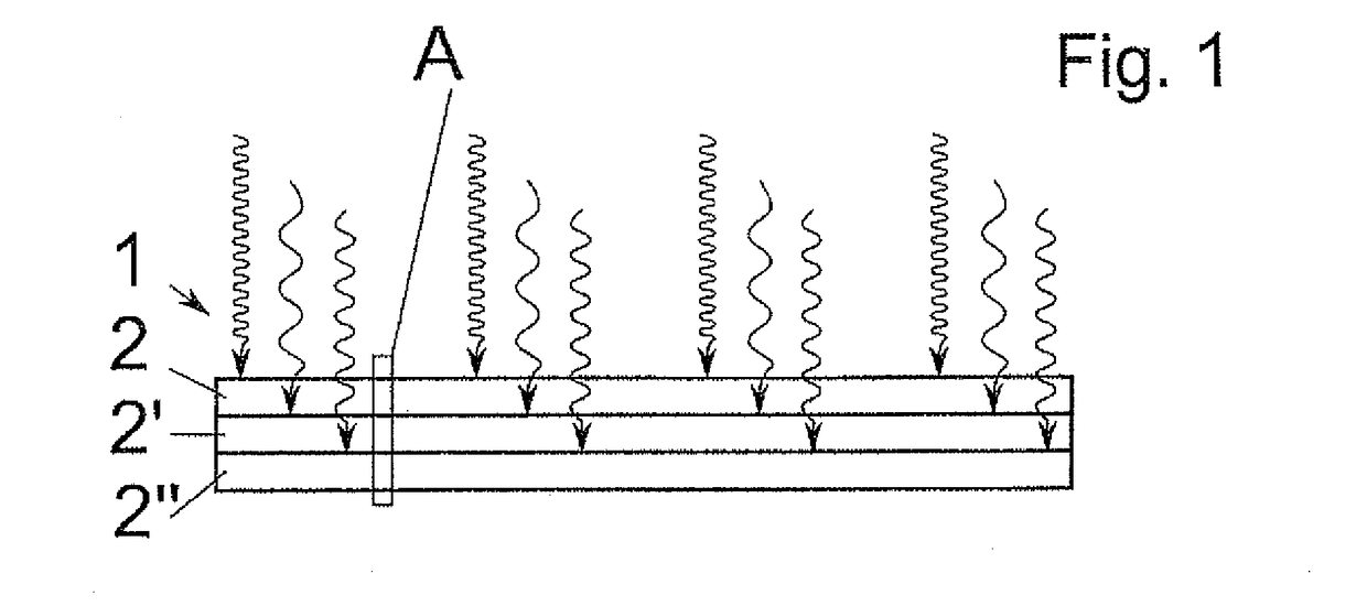
[0099]FIG. 2 shows an enlargement of the section A of the schematic cross-sectional view according to FIG. 1 in a first embodiment according to the invention, in which one can see dielectric layers, particularly oxide layers, 3, by means of which the substrates 2, 2′, 2″ have been connected to one another.

[0100]The dielectric layers 3 alternate in this case between the individual substrates 2, 2′, 2″. This alternation is preferably achieved in su...


PUM


Abstract

A method for producing a multiple-substrate stack from an, in particular wavelength-sensitive, semiconductor substrate and at least one further, in particular wavelength-sensitive, semiconductor substrate with the following steps: applying a dielectric layer, which is electrically conductive at least in certain sections, onto at least one substrate surface of at least one of the semiconductor substrates, and contacting the semiconductor substrate with the further semiconductor substrate and forming an electrically conductive connection between the semiconductor substrates.

Description

FIELD OF THE INVENTION[0001]The invention relates to a method for producing a multiple-substrate stack.BACKGROUND OF THE INVENTION[0002]There are diverse technical problems in the production of conductive multiple-substrate stacks, particularly for generating electricity:[0003]generating the greatest amount of electricity possible for the lowest possible area,[0004]mass production suitability for the lowest possible costs,[0005]long-term stability of the electricity generation,[0006]stability with respect to environmental influences, particularly at connection points,[0007]reliable electricity generation.[0008]The present invention is therefore based on the object of specifying a method, which at least partially, preferably predominantly, solves the aforementioned problems.SUMMARY OF THE INVENTION[0009]The object of the present invention is achieved with the features of the independent claim(s). Advantageous developments of the invention are specified in the dependent claims. All co...

Claims


Application Information

Patent Timeline
IPC IPC(8): H01L31/05H01L31/0224
CPCH01L31/022425H01L31/0512H01L31/043H01L21/187H01L25/043Y02E10/50H01L2924/0002H01L2924/00
Inventor MATTHIAS, THORSTEN
Owner EV GRP E THALLNER GMBH
Why Eureka
Try Eureka