

Semiconductor devices and methods of manufacturing the same
- Summary
- Abstract
- Description
- Claims
- Application Information
AI Technical Summary
Benefits of technology
Problems solved by technology
Method used
Image

Examples
Embodiment Construction
[0038]Reference will now be made to example embodiments, which are illustrated in the accompanying drawings, wherein like reference numerals may refer to like components throughout.
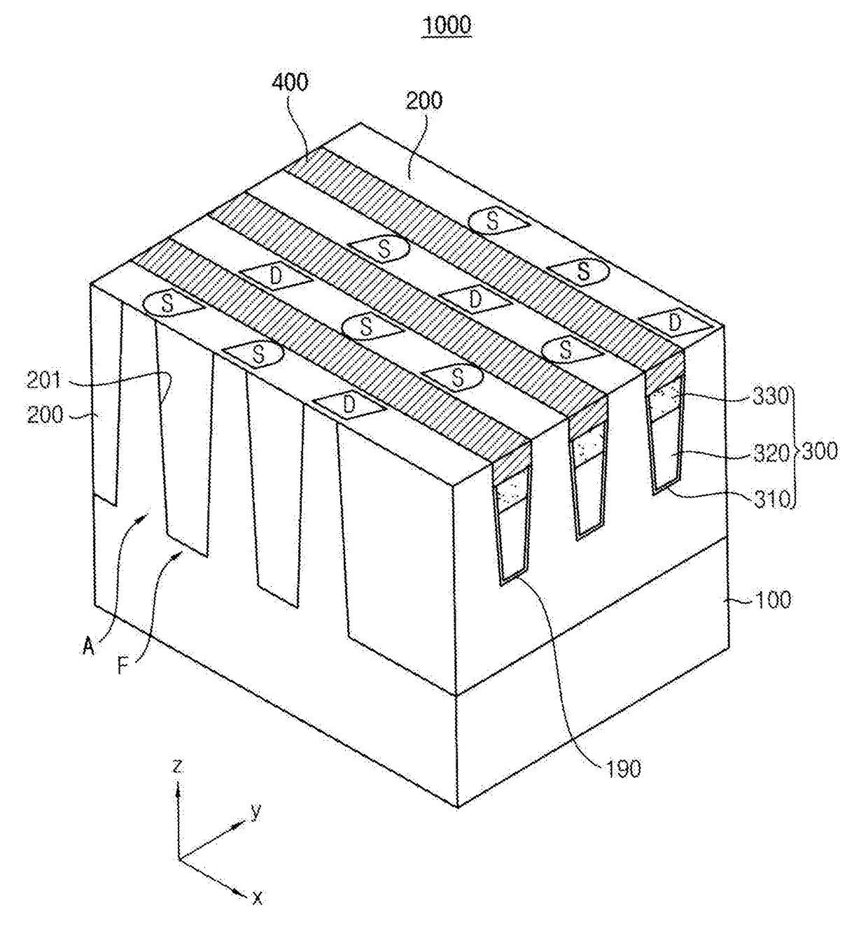
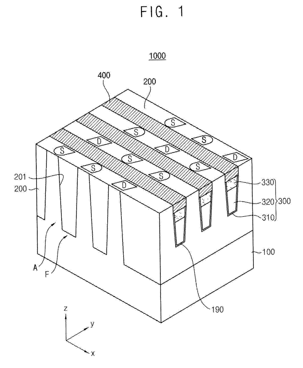
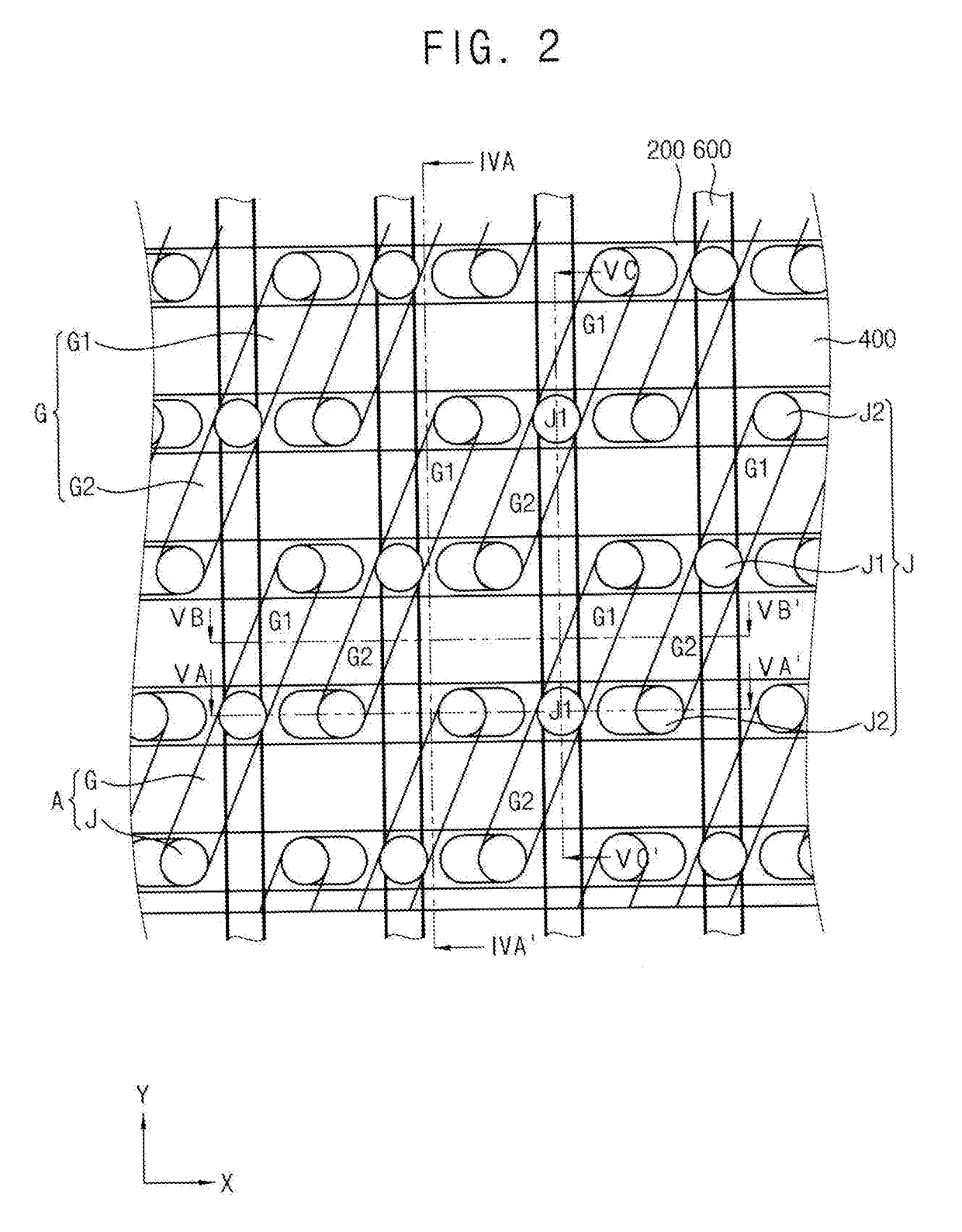
[0039]FIG. 1 is a perspective view illustrating a semiconductor device in accordance with some example embodiments of the present inventive concepts, and FIG. 2 is a layout of the semiconductor device shown in FIG. 1. FIG. 3 is a plan view of the semiconductor device shown in FIG. 1. FIG. 4A is a cross-sectional view of the semiconductor device shown in FIG. 1 cut along a line IVA-IVA′ of the layout shown in FIG. 2.
[0040]Referring to FIGS. 1 to 4A, the semiconductor device 1000 in accordance with some example embodiments may include a substrate 100 having an active region A defined by a device isolation layer 200 and at least one gate trench 190 linearly extending in a first direction x to cross the active region A, a first conductive line 300 located in the gate trench 190 and extending in the first dire...
PUM
 Abstract
Description
Claims
Application Information