Electronic Device and Method for Producing an Electronic Device

a technology of electronic devices and electronic components, applied in the direction of semiconductor devices, semiconductor/solid-state device details, electrical apparatus, etc., can solve the problems of gold layers, gold layers oxidizing over time, and putting the long-term stability of sintered connections at risk

Active Publication Date: 2017-09-21
OSRAM OLED
View PDF11 Cites 1 Cited by
  • Summary
  • Abstract
  • Description
  • Claims
  • Application Information

AI Technical Summary

Benefits of technology

[0019]According to another embodiment, the second component is an electronic semiconductor chip. The electronic semiconductor chip can be embodied as an optoelectronic semiconductor chip in the form of a light-emitting diode chip, laser diode chip or photo diode chip, for example. Moreover, the seco

Problems solved by technology

Since, on the one hand, sinter layers, e.g., of silver, may have a high solubility and diffusivity of oxygen, and, on the other hand, gold may dissolve in silver in the course of time, there is a risk that the ground below a gold cover layer oxidizes over time.
Experience has shown that a sinter layer eas

Method used


Image

  • Electronic Device and Method for Producing an Electronic Device
  • Electronic Device and Method for Producing an Electronic Device
  • Electronic Device and Method for Producing an Electronic Device

Examples


Embodiment Construction

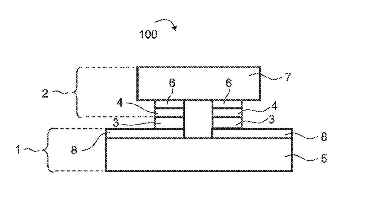
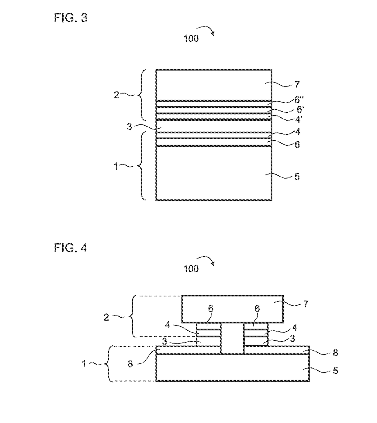
[0026]FIG. 1 shows an exemplary embodiment for an electronic device 100 comprising a first component 1 and a second component 2. A sinter layer 3 having a first metal is arranged between the first component 1 and the second component 2, the sinter layer connecting the first and second component 1, 2. For example, the first component 1 may be a carrier element and the second component 2 may be an electronic semiconductor chip, e.g., in the form of an optoelectronic semiconductor chip such as a light-emitting diode chip, a laser diode chip or a photo diode chip, or in the form or a power semiconductor component such as a transistor. Particularly preferably, the sinter layer 3 may comprise or be made of silver and / or copper.

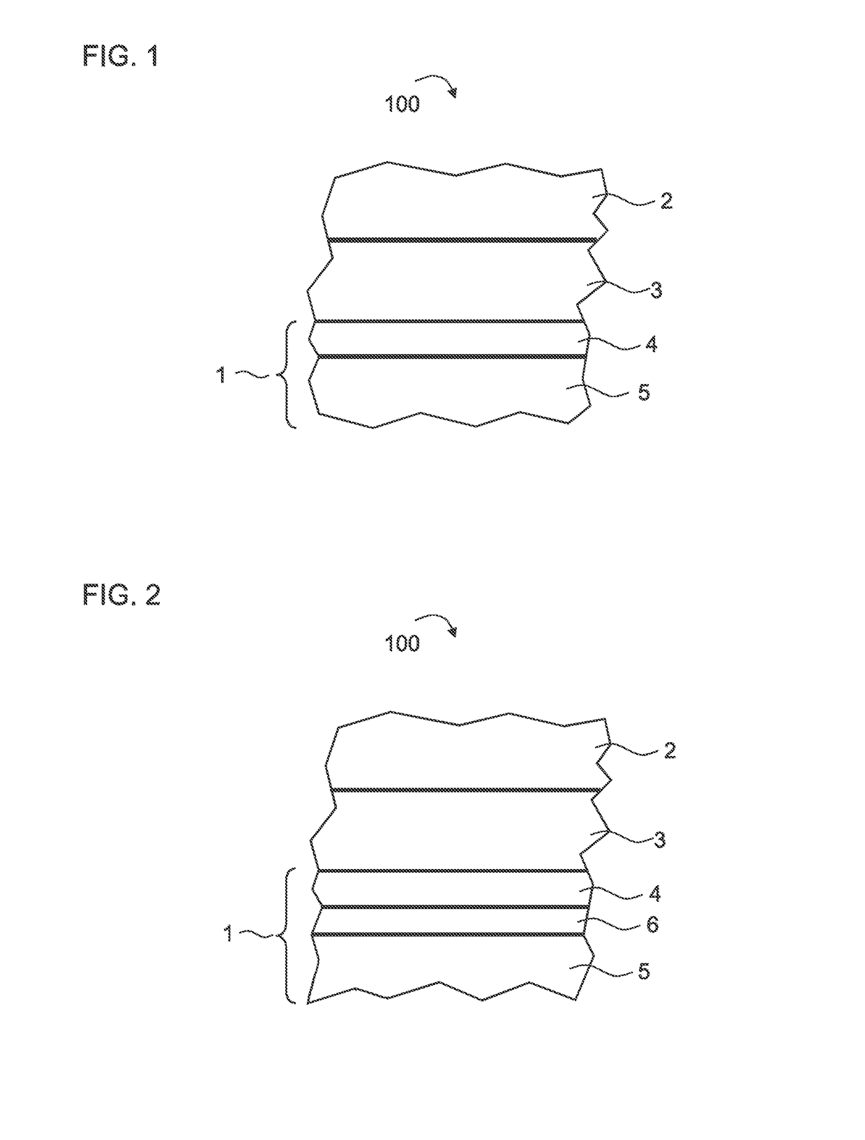
[0027]For the production of the electronic device 100, the first component 1 is provided. A sintering material is applied on the first component 1, which is applied in the form of a solvent-containing paste by means of a doctor blade or by printing, for example. The...


PUM


Abstract

An electronic device and a method for producing an electronic device are disclosed. In an embodiment the electronic device includes a first component and a second component and a sinter layer connecting the first component to the second component, the sinter layer comprising a first metal, wherein at least one of the components comprises at least one contact layer which is arranged in direct contact with the sinter layer, which comprises a second metal different from the first metal and which is free of gold.

Description

[0001]This patent application is a national phase filing under section 371 of PCT / EP2015 / 071356, filed Sep. 17, 2015, which claims the priority of German patent application 10 2014 115 319.7, filed Oct. 21, 2014, each of which is incorporated herein by reference in its entirety.TECHNICAL FIELD[0002]An electronic device and a method for producing an electronic device are provided. In particular, the electronic device comprises a sinter layer.BACKGROUND[0003]It is common for components, which are joined to one another by means of sintering, to comprise contact surfaces in the form of thin cover layers made of gold. For example, underlying layers that are prone to oxidation can be covered by means of such cover layers and thus be protected. Since, on the one hand, sinter layers, e.g., of silver, may have a high solubility and diffusivity of oxygen, and, on the other hand, gold may dissolve in silver in the course of time, there is a risk that the ground below a gold cover layer oxidize...

Claims


Application Information

Patent Timeline
IPC IPC(8): H01L23/00H01L23/498H01L23/15
CPCH01L24/29H01L2924/10349H01L23/49866H01L24/83H01L24/32H01L2224/29139H01L2224/29147H01L2224/83192H01L2224/8384H01L2224/83359H01L2224/83439H01L2224/83447H01L2224/83469H01L2224/83473H01L2224/83478H01L2924/12041H01L2924/15724H01L2224/29084H01L2224/29083H01L2224/29124H01L2224/29155H01L2224/29166H01L2224/29171H01L2224/29169H01L2224/29173H01L2224/29178H01L2224/32503H01L2924/13064H01L2924/1033H01L23/15H01L33/40H01L33/62H01L2224/83208H01L2924/12042H01L2224/27334H01L24/03H01L24/05H01L24/11H01L24/13H01L24/16H01L24/27H01L24/81H01L2224/0345H01L2224/0401H01L2224/04026H01L2224/05082H01L2224/05124H01L2224/05155H01L2224/05166H01L2224/05171H01L2224/05669H01L2224/05673H01L2224/05678H01L2224/1132H01L2224/11334H01L2224/1141H01L2224/11436H01L2224/13294H01L2224/13339H01L2224/13347H01L2224/16227H01L2224/16245H01L2224/2732H01L2224/2741H01L2224/27436H01L2224/29339H01L2224/29347H01L2224/32227H01L2224/32245H01L2224/73265H01L2224/81191H01L2224/81192H01L2224/81193H01L2224/81201H01L2224/81203H01L2224/81205H01L2224/81207H01L2224/81208H01L2224/81469H01L2224/81473H01L2224/81478H01L2224/8184H01L2224/83191H01L2224/83193H01L2224/83201H01L2224/83203H01L2224/83205H01L2224/83207H01L2924/00015H01L2924/12043H01L2224/29294H01L2924/13014H01L2924/00014H01L2224/05644H01L2224/05639H01L2924/00012H01L24/15H01L23/49513
Inventor PLOESSL, ANDREAS
Owner OSRAM OLED
Why Eureka
Try Eureka