Eureka AIR delivers breakthrough ideas for toughest innovation challenges, trusted by R&D personnel around the world.

Wafer processing method

Active Publication Date: 2017-10-19
DISCO CORP
View PDF4 Cites 7 Cited by
  • Summary
  • Abstract
  • Description
  • Claims
  • Application Information

AI Technical Summary

Benefits of technology

The present invention provides a method for processing wafers by removing the annular reinforcing portion from the wafer. By using a laser beam to separate the annular reinforcing portion from the device area, the method ensures proper alignment of the wafer even after removing the reinforcing portion. A mark is formed on the wafer to indicate the position of the notch formed on the reinforcing portion, which helps in aligning the wafer during the subsequent step. This method simplifies the processing process and improves the quality of wafers.

Problems solved by technology

However, in the wafer processing method described in Japanese Patent Laid-open No. 2015-147231, there is a problem such that when the annular reinforcing portion is removed from the wafer, a notch formed on the annular reinforcing portion is also removed from the wafer, so that alignment for the wafer in a subsequent step becomes difficult.

Method used


Image

  • Wafer processing method
  • Wafer processing method
  • Wafer processing method

Examples


Embodiment Construction

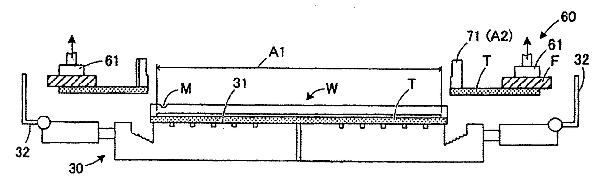
[0020]A wafer processing method according to a preferred embodiment of the present invention will now be described with reference to the attached drawings. FIG. 1 is a perspective view of a laser processing apparatus 1 for use in performing the wafer processing method according to this preferred embodiment. The configuration of the laser processing apparatus 1 shown in FIG. 1 is merely illustrative, and any other configurations may be used in performing the wafer processing method according to this preferred embodiment.

[0021]As shown in FIG. 1, the laser processing apparatus 1 includes laser beam applying means 40 for applying a laser beam to a wafer W held on a holding table 30, wherein the laser beam applying means 40 and the holding table 30 are relatively moved to process the wafer W. A plurality of crossing division lines (not shown) are formed on the front side of the wafer W to thereby define a plurality of separate regions where a plurality of devices (not shown) are formed....


PUM


Abstract

Disclosed herein is a wafer processing method for removing an annular reinforcing portion from a wafer having a device area, the annular reinforcing portion being formed around the device area. The wafer processing method includes the steps of supporting the wafer through an adhesive tape to an annular frame, forming a mark corresponding to a notch at a position radially inside a boundary portion between the annular reinforcing portion and the device area, cutting the boundary portion together with the adhesive tape to thereby separate the annular reinforcing portion from the device area, and moving the annular reinforcing portion supported through the adhesive tape to the annular frame away from a holding table to thereby remove the annular reinforcing portion from the wafer.

Description

BACKGROUND OF THE INVENTIONField of the Invention[0001]The present invention relates to a wafer processing method for removing an annular reinforcing portion from a wafer having a device area, the annular reinforcing portion being formed around the device area.Description of the Related Art[0002]A wafer having a plurality of devices such as integrated circuits (ICs) and large scale integrations (LSIs) on the front side is divided into a plurality of individual chips corresponding to the plural devices by using a dicing apparatus or the like. These chips are widely used so as to be built in various electronic equipment. For the purposes of reducing the size and weight of electronic equipment, the thickness of the wafer is reduced to 50 to 100 μm, for example. However, such a thin wafer has low rigidity, and warpage may also occur. Accordingly, the wafer is difficult to handle. To cope with this problem, there has been proposed a method of grinding the back side of the wafer in a cent...

Claims


Application Information

Patent Timeline
IPC IPC(8): H01L21/67H01L23/544H01L21/683H01L21/66
CPCH01L21/67115H01L23/544H01L21/6836H01L22/20H01L2223/54426H01L2223/54453H01L2223/54493H01L2221/68381B23K26/38H01L21/302H01L21/67132H01L2223/544B23K26/702B23K26/032B23K26/0823B23K26/0846H01L21/78H01L2221/68327H01L21/68721H01L21/6835
Inventor TSUCHIYA, TOSHIOHOSHINO, HITOSHI
Owner DISCO CORP
Why Eureka
Eureka Blog
Learn More