Semiconductor apparatus, production method, and electronic apparatus

a technology of electromagnetic radiation and production method, applied in the direction of radio frequency controlled devices, instruments, television systems, etc., can solve the problems of lowering the velocity and increasing the power consumption, increasing the waste area of chips, and reducing the assembly throughpu

Active Publication Date: 2017-11-02
SONY CORP
View PDF17 Cites 13 Cited by
  • Summary
  • Abstract
  • Description
  • Claims
  • Application Information

AI Technical Summary

Benefits of technology

[0038]According to the aspect of the present technology, array devices that are the same can be created using the same mask set, and a 3D network in which the array devices are electrically con

Problems solved by technology

However, since an impedance of the input/output terminal and protection device is large, lowering of a velocity and an increase of power consumption become a problem.
Moreover, since

Method used


Image

  • Semiconductor apparatus, production method, and electronic apparatus
  • Semiconductor apparatus, production method, and electronic apparatus
  • Semiconductor apparatus, production method, and electronic apparatus

Examples


application example

[0075]8. Regarding application example

[0076]9. Regarding application example (memory)

[0077]10. Regarding electronic apparatus

[0078]11. Regarding usage example of image pickup apparatus

[0079]

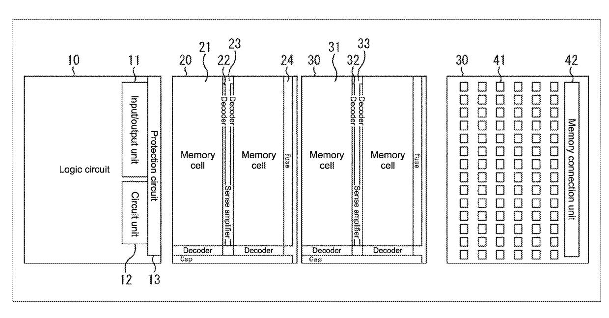
[0080]According to the present technology, it is possible to provide, in a semiconductor device in which array devices that are the same are created using the same mask set and are electrically connected to one another, a semiconductor apparatus whose arrangement address in a longitudinal (Z-axis) direction of a laminated device is identified by writing of potentials using external signals.

[0081]A structure of a device including an array arrangement, such as a memory and a gate array, can use its multilayer structure for scale expansion. Therefore, the same mask set can be shared and used by a plurality of device sets. Here, descriptions will be given while taking a semiconductor apparatus including such a device structure as an example.

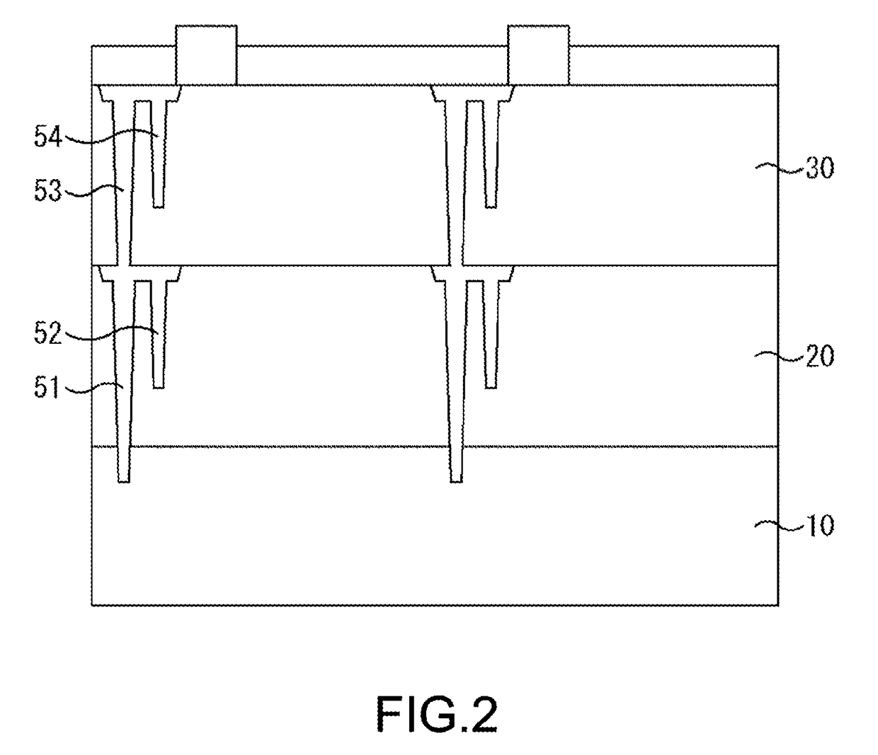
[0082]Referring to FIGS. 1 and 2, a semiconductor apparatus ...


PUM


Abstract

The present technology relates to a semiconductor apparatus, a production method, and an electronic apparatus that enable semiconductor apparatuses to be laminated and the laminated semiconductor apparatuses to be identified. A semiconductor apparatus that is laminated and integrated with a plurality of semiconductor apparatuses, includes a first penetrating electrode for connecting with the other semiconductor apparatuses and a second penetrating electrode that connects the first penetrating electrode and an internal device, the second penetrating electrode being arranged at a position that differs for each of the laminated semiconductor apparatuses. The second penetrating electrode indicates a lamination position at a time of lamination. An address of each of the laminated semiconductor apparatuses in a lamination direction is identified by writing using external signals after lamination. The present technology is applicable to a memory chip and an FPGA chip.

Description

TECHNICAL FIELD[0001]The present technology relates to a semiconductor apparatus, a production method, and an electronic apparatus, more particularly, to a semiconductor apparatus obtained by laminating and integrating devices such as a memory, a logic circuit, and an FPGA (Field-Programmable Gate Array), a production method, and an electronic apparatus.BACKGROUND ART[0002]Semiconductor apparatuses such as a memory are desired to be made compact in view of yields and package sizes, and a semiconductor device obtained by electrically connecting and integrating segmentalized semiconductor chips is already mass-produced.[0003]Such a semiconductor apparatus is realized as a developed variation of mainly a package technology, and a method of connecting via an electrode on a chip side wall, a method of connecting via a silicon interposer, a method of connecting via a penetrating electrode, and the like are exemplified as an application example.[0004]In a case where chips are electrically ...

Claims


Application Information

Patent Timeline
IPC IPC(8): H01L25/065H03K19/0175H01L25/18H01L27/146G11C5/06G11C5/02H01L23/528H01L23/48H01L21/768G11C8/10G11C7/10H04N5/907H01L27/118
CPCH01L23/528H03K19/017581H01L21/76898H01L27/118H01L27/14636H01L25/18H04N5/907H01L2225/06541H01L25/0657G11C5/02G11C7/1012G11C8/10G11C5/06H01L23/481H01L27/14634G06F12/00G11C5/00G11C29/00H01L27/146H01L2924/0002G11C5/025G11C7/16G11C29/70H04N5/772H01L2225/06544H01L2225/06565H04N23/555H04N25/75H01L2924/00H01L25/065H01L25/07H01L23/4824H01L23/4825H01L25/0756H01L23/48H01L25/117H01L25/043H01L23/485H01L21/76897H01L25/04
Inventor TAKAHASHI, HIROSHIARAKAWA, TOMOFUMIISHIDA, MINORU
Owner SONY CORP
Why Eureka
Try Eureka