Optoelectronic Semiconductor Device and Apparatus with an Optoelectronic Semiconductor Device

a technology of optoelectronic semiconductor and semiconductor device, which is applied in the direction of semiconductor devices, electrical equipment, basic electric elements, etc., can solve the problems of device inability to be used in applications in which esd protection diodes have a disruptive effect or at least unwanted effects

Active Publication Date: 2017-11-02
OSRAM OLED
View PDF10 Cites 2 Cited by
  • Summary
  • Abstract
  • Description
  • Claims
  • Application Information

AI Technical Summary

Benefits of technology

[0025]According to at least one embodiment of the semiconductor device, a surface of the first contact region facing away from the carrier is located at the same distance or substantially at the same distance from the carrier as a surface of the second contact region facing away from the carrier. “Substantially at the same distance” means that the distances differ from one another by at most 5 μm. The difference preferably amounts to at most 2 μm, particularly preferably at most 1 μm. In other words, the surfaces of the first contact region and of the second contact region facing away from the carrier form a common plane. Simultaneous electrical contacting of the first contact region and the second contact region by means of a connecting lead is consequently simplified.

Problems solved by technology

In optoelectronic semiconductor devices such as, for example, light-emitting diodes, there is the risk of irreparable damage occurring due to an electrostatic discharge (ESD) during transport or also during processing of the devices.
Such devices cannot, however, be used in applications in which ESD protection diodes have a disruptive effect or are at least unwanted.

Method used


Image

  • Optoelectronic Semiconductor Device and Apparatus with an Optoelectronic Semiconductor Device
  • Optoelectronic Semiconductor Device and Apparatus with an Optoelectronic Semiconductor Device
  • Optoelectronic Semiconductor Device and Apparatus with an Optoelectronic Semiconductor Device

Examples


Embodiment Construction

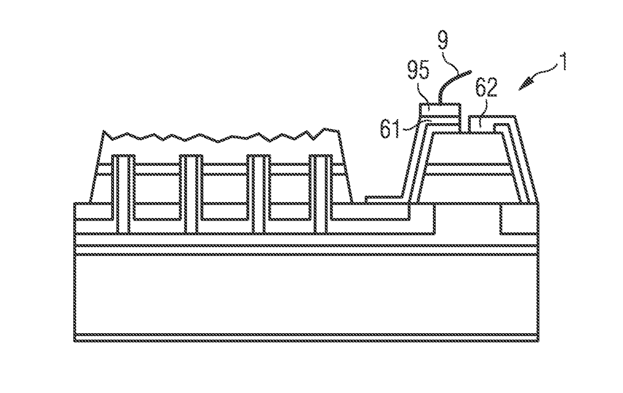
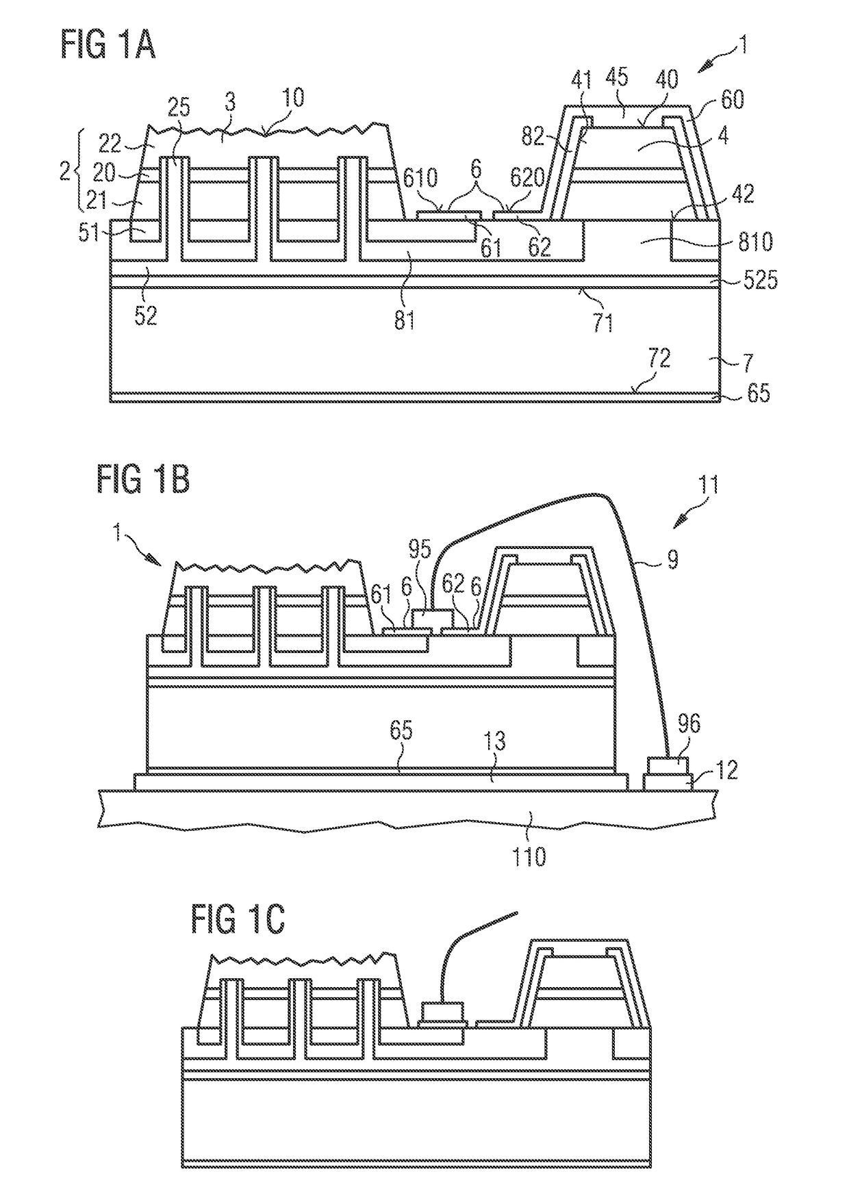
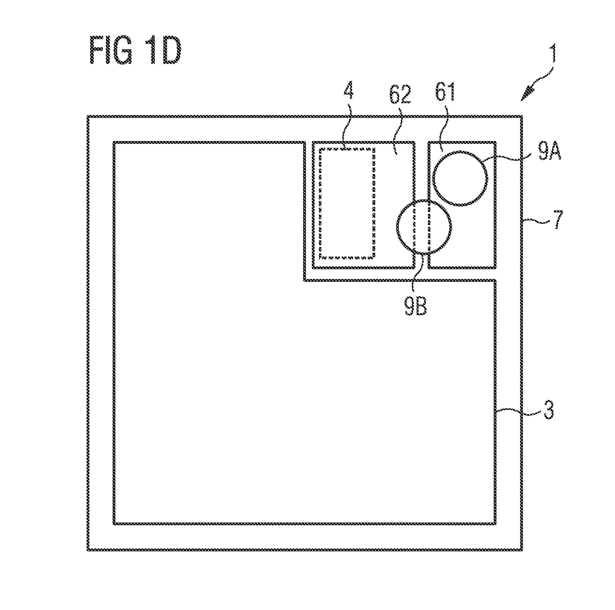
[0037]FIG. 1A shows a schematic sectional view of an exemplary embodiment of an optoelectronic semiconductor device 1. The semiconductor device 1 comprises an emission region 3. The emission region comprises a semiconductor layer sequence 2 with an active region 20 for generating radiation. The active region 20 is arranged between a first semiconductor layer 21 of a first conduction type and a second semiconductor layer 22 of a second conduction type different from the first conduction type. For example, the first semiconductor layer is p-conductive and the second semiconductor layer n-conductive.

[0038]The semiconductor device 1 furthermore comprises a protection diode region 4. In the exemplary embodiment shown, the protection diode region takes the form of a semiconductor body which, during production of the semiconductor device, originates from the same semiconductor layer sequence 2 as the emission region 3. The protection diode region 4 thus likewise comprises an active region ...


PUM


Abstract

An optoelectronic semiconductor device and an apparatus with an optoelectronic semiconductor device are disclosed. In an embodiment the optoelectronic semiconductor component has an emission region including a semiconductor layer sequence having a first semiconductor layer, a second semiconductor layer, and an active region arranged between the first semiconductor layer and the second semiconductor layer for generating radiation, and a protection diode region. The semiconductor component has a contact for electrically contacting the semiconductor component externally. The contact has a first contact region that is connected to the emission region in an electrically conductive manner. The contact has further a second contact region that is spaced apart from the first contact region and connected to the protection diode region in an electrically conductive manner. The first contact region and the second contact region can be electrically contacted externally by a mutual end of a connecting line.

Description

[0001]This patent application is a national phase filing under section 371 of PCT / EP2015 / 074353, filed Oct. 21, 2015, which claims the priority of German patent application 10 2014 116 512.8, filed Nov. 12, 2014, each of which is incorporated herein by reference in its entirety.TECHNICAL FIELD[0002]The present application relates to an optoelectronic semiconductor device and an apparatus with an optoelectronic semiconductor device.BACKGROUND[0003]In optoelectronic semiconductor devices such as, for example, light-emitting diodes, there is the risk of irreparable damage occurring due to an electrostatic discharge (ESD) during transport or also during processing of the devices. It is estimated that approx. 8 to 33% of electronic component failures are attributable to such ESD damage. ESD protection diodes may be integrated into the devices in order to avoid such damage. Such devices cannot, however, be used in applications in which ESD protection diodes have a disruptive effect or are...

Claims


Application Information

Patent Timeline
Patent Type & Authority Applications(United States)
IPC IPC(8): H01L27/02H01L33/38H01L27/15H01L33/62H01L33/40
CPCH01L27/0248H01L27/15H01L33/405H01L33/382H01L33/387H01L33/62H01L2224/73265H01L2224/48227H01L33/38
Inventor MOOSBURGER, JUERGENPLOESSL, ANDREAS
Owner OSRAM OLED
Why Eureka
Try Eureka