
Method of manufacturing memory device

a memory device and manufacturing method technology, applied in the direction of semiconductor devices, basic electric elements, electrical appliances, etc., can solve the problems of volatile memory devices losing data stored therein, and achieve the effect of improving the charge storage capacity of memory cells

Inactive Publication Date: 2017-11-16
SK HYNIX INC
View PDF0 Cites 19 Cited by
  • Summary
  • Abstract
  • Description
  • Claims
  • Application Information

AI Technical Summary

Benefits of technology

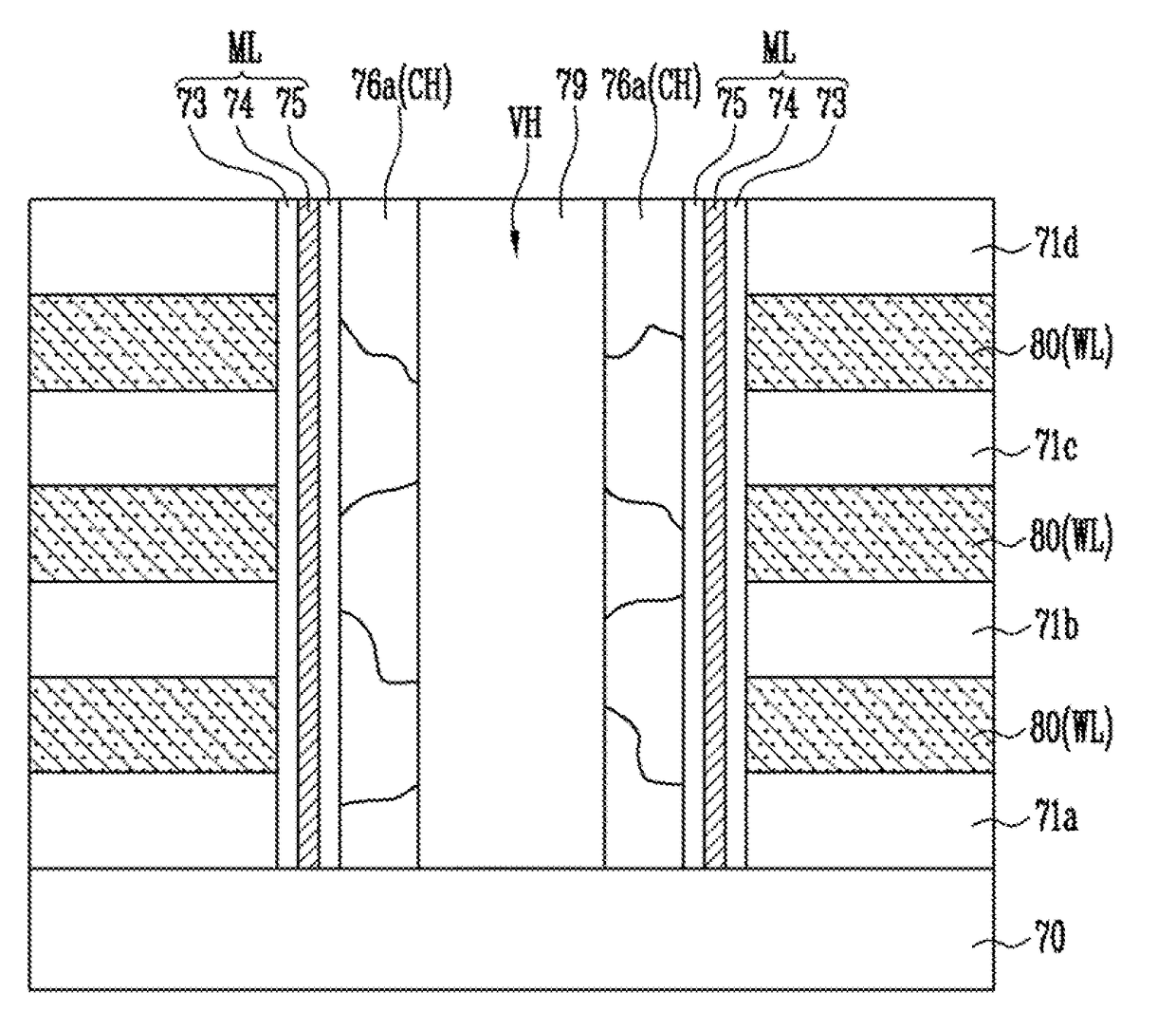
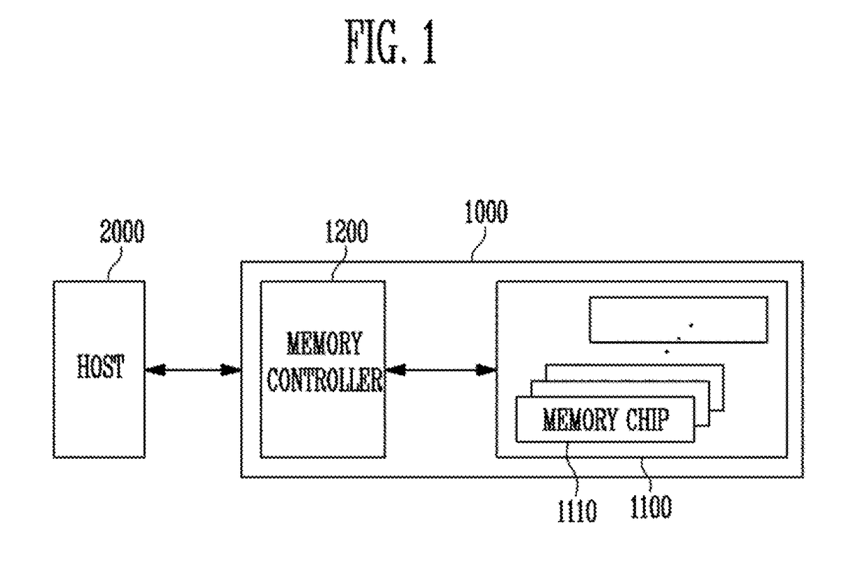
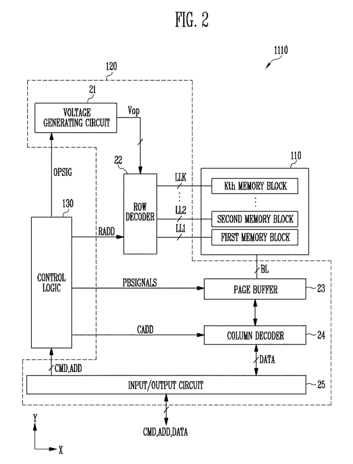
The present patent is about a method for making a memory device that can increase the capacity of memory cells in a three-dimensional memory device.

Problems solved by technology

A volatile memory device loses data stored therein when a power supply is cut off.

Method used


Image

  • Method of manufacturing memory device
  • Method of manufacturing memory device
  • Method of manufacturing memory device

Examples


Embodiment Construction

[0021]Hereinafter, embodiments will be described in greater detail with reference to the accompanying drawings. Embodiments are described herein with reference to cross-sectional illustrations that are schematic illustrations of embodiments (and intermediate structures). As such, variations from the shapes of the Illustrations as a result, for example, of manufacturing techniques and / or tolerances, are to be expected. Thus, embodiments should not be construed as limited to the particular shapes of regions illustrated herein but may include deviations in shapes that result, for example, from manufacturing. In the drawings, lengths and sizes of layers and regions may be exaggerated for clarity. Like reference numerals in the drawings denote like elements.

[0022]Terms such as ‘first’ and ‘second’ may be used to describe various components, but they should not limit the various components. Those terms are only used for the purpose of differentiating a component from other components. For...


PUM


Abstract

Provided herein is a method of manufacturing a memory device. The method of manufacturing the memory device includes: forming a compensation layer over the channel layer, wherein an incubation time used for a nucleation of the compensation layer is shorter than an incubation time of the channel layer; and performing a heat treatment process for crystallizing the channel layer.

Description

CROSS-REFERENCE TO RELATED APPLICATION[0001]The present application claims priority under 35 U.S.C. 119(a) to Korean patent application number 10-2016-0058347 filed on May 12, 2016, which is incorporated herein by reference in its entirety.BACKGROUND1. Field[0002]Various embodiments of the present disclosure relate to a method of manufacturing a memory device, and more particularly, to the method of manufacturing a three-dimensional memory device.2. Description of the Related Art[0003]Generally, memory devices may be classified into volatile memory devices and nonvolatile memory devices. A volatile memory device loses data stored therein when a power supply is cut off. On the other hand, a nonvolatile memory device retains data stored therein even if a power supply is cut off. Due to this, the nonvolatile memory device has been widely used as a portable storage device.[0004]A memory device may include a memory cell array for storing data, a peripheral circuit for performing a progra...

Claims


Application Information

Patent Timeline
Patent Type & Authority Applications(United States)
IPC IPC(8): H01L21/02H01L21/306H01L27/11582H01L21/324
CPCH01L21/02667H01L21/02532H01L21/02592H01L21/324H01L21/30604H01L27/11582H10B43/35H10B43/27H10B41/23H10B43/23H10B41/27
Inventor KIM, JIN HA
Owner SK HYNIX INC
Learn More