Preparation method of non-volatile charge storage device, non-volatile charge storage device and application of device

A charge storage and device technology, applied in the field of microelectronic materials, can solve the problems of unbearable device leakage current, inability to function as an insulating medium, and poor data retention performance

Inactive Publication Date: 2011-11-02
NANJING UNIV
View PDF2 Cites 9 Cited by
  • Summary
  • Abstract
  • Description
  • Claims
  • Application Information

AI Technical Summary

Problems solved by technology

However, studies have shown that using nitride (Si 3 N 4 ) as the storage layer of the charge storage device has poor data retention performance, while the traditional SiO 2 The thickness of the tunneling layer and the barrier layer is getting thinner and thinner, and the tunneling current increases rapidly due to the quantum tunneling effect, resulting in SiO 2 The layer cannot play the role of insulating medium, and the leakage current of the device has reached an unbearable level

Method used


Image

  • Preparation method of non-volatile charge storage device, non-volatile charge storage device and application of device
  • Preparation method of non-volatile charge storage device, non-volatile charge storage device and application of device
  • Preparation method of non-volatile charge storage device, non-volatile charge storage device and application of device

Examples


Embodiment 1

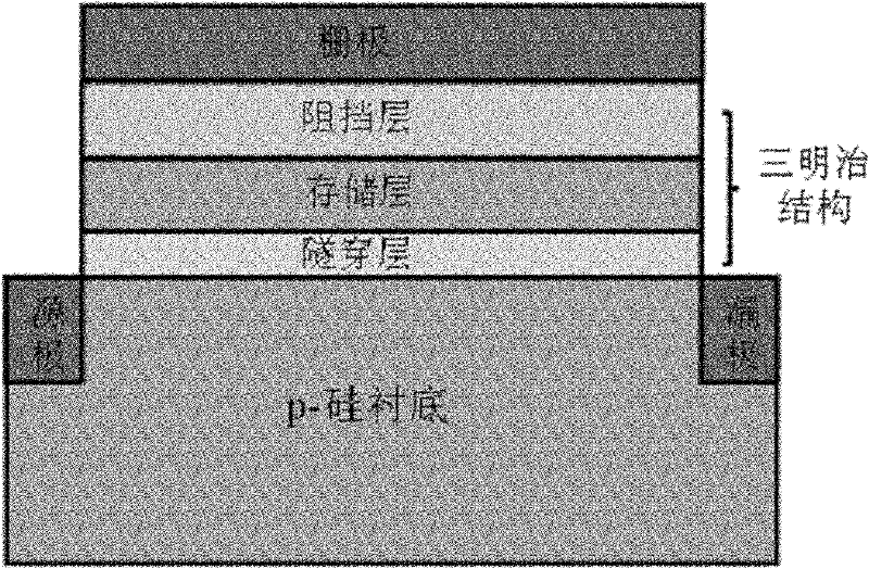
[0033] Example 1: Based on p-Si substrate, Si / Al 2 O 3 / (HfO 2 ) 0.8 (Al 2 O 3 ) 0.2 / Al 2 O 3 The preparation process of the / Pt charge storage device is as follows:

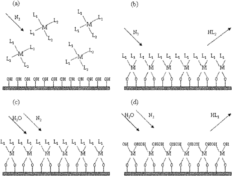
[0034] (a) Put the p-Si substrate into an appropriate amount of acetone, and after ultrasonic cleaning, ultrasonically clean with deionized water to rinse away the remaining impurities on the surface of the substrate. The substrate is then immersed in hydrofluoric acid to remove surface oxides, and then ultrasonically cleaned with deionized water, dried with high-purity nitrogen, and placed in an atomic layer chemical vapor deposition chamber to prepare a thin film.

[0035] (b) Using HfCl during the deposition process 4 And Al(CH 3 ) 3 As the metal source, water is the oxygen source. Al(CH 3 ) 3 As the nitrogen enters the cavity, it reacts with the surface of the silicon substrate at the hydroxyl terminal and reaches saturation. After that, the oxygen source is brought into the cavity by the nitrogen and reacts wit...

Embodiment 1

[0041] Comparative Example 1: Based on p-Si substrate, Si / Al 2 O 3 / HfO 2 / Al 2 O 3 The preparation process of the / Pt charge storage device is as follows:

[0042] (a) Put the p-Si substrate into an appropriate amount of acetone, and after ultrasonic cleaning, ultrasonically clean with deionized water to rinse away the remaining impurities on the surface of the substrate. The substrate is then immersed in hydrofluoric acid to remove surface oxides, and then ultrasonically cleaned with deionized water, dried with high-purity nitrogen, and placed in an atomic layer chemical vapor deposition chamber to prepare a thin film.

[0043] (b) Using HfCl during the deposition process 4 And Al(CH 3 ) 3 As the metal source, water is the oxygen source. Al(CH 3 ) 3 As the nitrogen enters the cavity, it reacts with the surface of the silicon substrate at the hydroxyl terminal and reaches saturation. After that, the oxygen source is brought into the cavity by the nitrogen and reacts with the metal...

Embodiment 2

[0049] Example 2: Based on p-Si substrate, Si / Al with different tunneling layer thicknesses 2 O 3 / (HfO 2 ) 0.8 (Al 2 O 3 ) 0.2 / Al 2 O 3 The preparation process of the / Pt charge storage device is as follows:

[0050] (a) Put the p-Si substrate into an appropriate amount of acetone, and after ultrasonic cleaning, ultrasonically clean with deionized water to rinse away the remaining impurities on the surface of the substrate. The substrate is then immersed in hydrofluoric acid to remove surface oxides, and then ultrasonically cleaned with deionized water, dried with high-purity nitrogen, and placed in an atomic layer chemical vapor deposition chamber to prepare a thin film.

[0051] (b) Using HfCl during the deposition process 4 And Al(CH 3 ) 3 As the metal source, water is the oxygen source. Al(CH 3 ) 3 As the nitrogen enters the cavity, it reacts with the surface of the silicon substrate at the hydroxyl terminal and reaches saturation. After that, the oxygen source is brought int...


PUM


Abstract

The invention relates to a preparation method of a non-volatile charge storage device, the non-volatile charge storage device and application thereof. The preparation method of the non-volatile charge storage device comprises the following specific steps: a) precipitating Al2O3 on the surface of a substrate by use of an atomic layer chemical vapor deposition method so as to form a tunneling layer; b) precipitating a layer of (HfO2)x(Al2O3)1-x film serving as a storage layer on the surface of the tunneling layer by use of the atomic layer chemical vapor deposition method; and c) precipitating a layer of Al2O3 serving as a barrier layer on the surface of the (HfO2)x(Al2O3)1-x storage layer by use of the chemical vapor deposition method. The non-volatile charge storage device comprises the tunneling layer, the storage layer and the barrier layer which are successively connected; Al2O3 is used as the tunneling layer and barrier layer of the storage device, and (HfO2)x(Al2O3)1-x is used asthe storage layer of the device. By using the method, the writing-in and erasing speeds of the device can be well improved, and simultaneously, the preparation method is simple to operate and easy tocontrol.

Description

Technical field [0001] The invention relates to a non-volatile charge storage device, a preparation method and application thereof, and belongs to the field of microelectronic materials. Background technique [0002] For decades, the development of integrated circuits has basically followed the Moore’s Law predicted by Dr. Gordon E. Moore, one of the founders of Intel Corporation, in 1964: the number of components integrated on a single chip of an integrated circuit, that is, the degree of integration of the integrated circuit, Doubled in 12 to 18 months, feature size reduced Times. As the feature size of the device becomes smaller and smaller, the traditional floating gate type non-volatile semiconductor memory device faces serious leakage problems. The size of the tunneling layer in floating gate memory devices is continuously reduced, so that a single defect will cause all the charges stored in the polysilicon floating gate to be lost. To solve this problem, polysilicon-oxi...

Claims


Application Information

Patent Timeline
Patent Type & Authority Applications(China)
IPC IPC(8): H01L21/336H01L21/285H01L29/792H01L29/51
Inventor 汤振杰刘治国殷江夏奕东李爱东
Owner NANJING UNIV
Why Eureka
Try Eureka