

Double pinned photodiode for CMOS APS and method of formation
a photodiode and cmos technology, applied in the field of semiconductor devices, can solve problems such as image lag and inadequate photosignal, and achieve the effect of increasing the charge storage capacity of the photodiod
- Summary
- Abstract
- Description
- Claims
- Application Information
AI Technical Summary
Benefits of technology
Problems solved by technology
Method used
Image

Examples
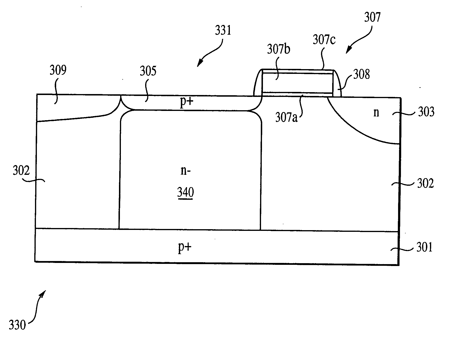
embodiment 331
[0053] Therefore, the pinned photodiode of embodiment 331 is effective at very small photodiode dimensions, 1 micron×1 micron and below; for semiconductor materials having a higher absorption coefficient than silicon in the visible wavelength range, such as silicon-germanium alloy or semiconductors of III-V material system; and / or when some quantum efficiency loss is acceptable.
[0054] In addition to increased charge capacity, this embodiment may reduce dark current and cross-talk. Dark current should be reduced because to achieve a same electron storage capacity, photodiode 331 will make better use of the pixel volume it occupies and, therefore, may have a lower n− concentration. In an abrupt p+ / n− junction, the lower doped side will determine the junction leakage. Also, cross-talk may be prevented because the n− region 340 extends to the substrate base collecting electrons in an area closer to the substrate base 301, which in a conventional photodiode, may diffuse into another pixe...
second embodiment
[0055]FIG. 6 depicts a more complex second embodiment of a pinned photodiode 661 in accordance with the invention. Photodiode 661 is located between a gate 607 of a transfer transistor and a STI region 609, and includes an intermediate p− region 670 partially separating a surface n− region 651 and a base n− region 652, which remain connected along edges thereof. The surface n− region 651 forms a junction with a p+ surface layer 605, and the base n− region 652 forms a junction with the p+ substrate base 601.
[0056] Formation of the pinned photodiode 661 will be described with reference to FIGS. 7A-7E. Referring to FIG. 7A, a substrate base 601 of a first conductivity type is provided. The substrate base 601 may be provided with the wafer. Instead of a substrate base 601 of a first conductivity type, there may be a base layer of a first conductivity type that is implanted beneath the photodiode 661 by conventional methods before or after the formation of photodiode 661. For simplicity,...
PUM
 Abstract
Description
Claims
Application Information