Antenna with micro-transfer-printed circuit element

Active Publication Date: 2017-11-23
X CELEPRINT LIMITED
View PDF8 Cites 18 Cited by
  • Summary
  • Abstract
  • Description
  • Claims
  • Application Information

AI Technical Summary

Benefits of technology

[0021]The present invention provides structures and methods that enable the construction of circuit elements that are transfer printed onto a device substrate and electrically connected using connection posts. The micro-transfer printing process enables the use of smalle

Problems solved by technology

Thus, such communication devices are relatively large and readily visible to an observer.
This process is expensive and requires a number of manufacturing steps.
Moreover, the topographical structure of the small integrated circuits over the destination substrate renders the electrical connections problematic.
For example, it can be diffic

Method used


Image

  • Antenna with micro-transfer-printed circuit element
  • Antenna with micro-transfer-printed circuit element
  • Antenna with micro-transfer-printed circuit element

Examples


Embodiment Construction

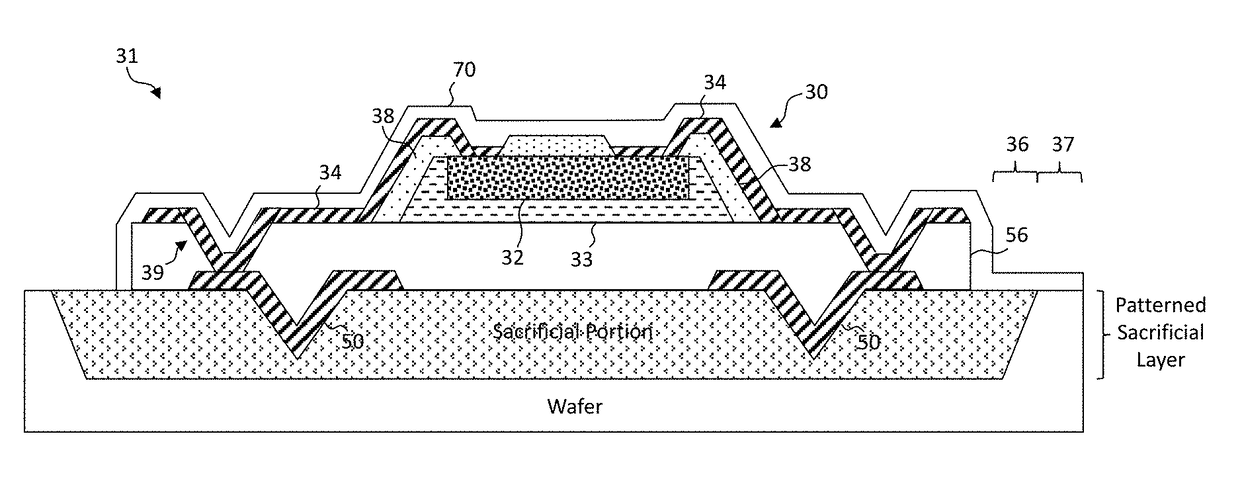
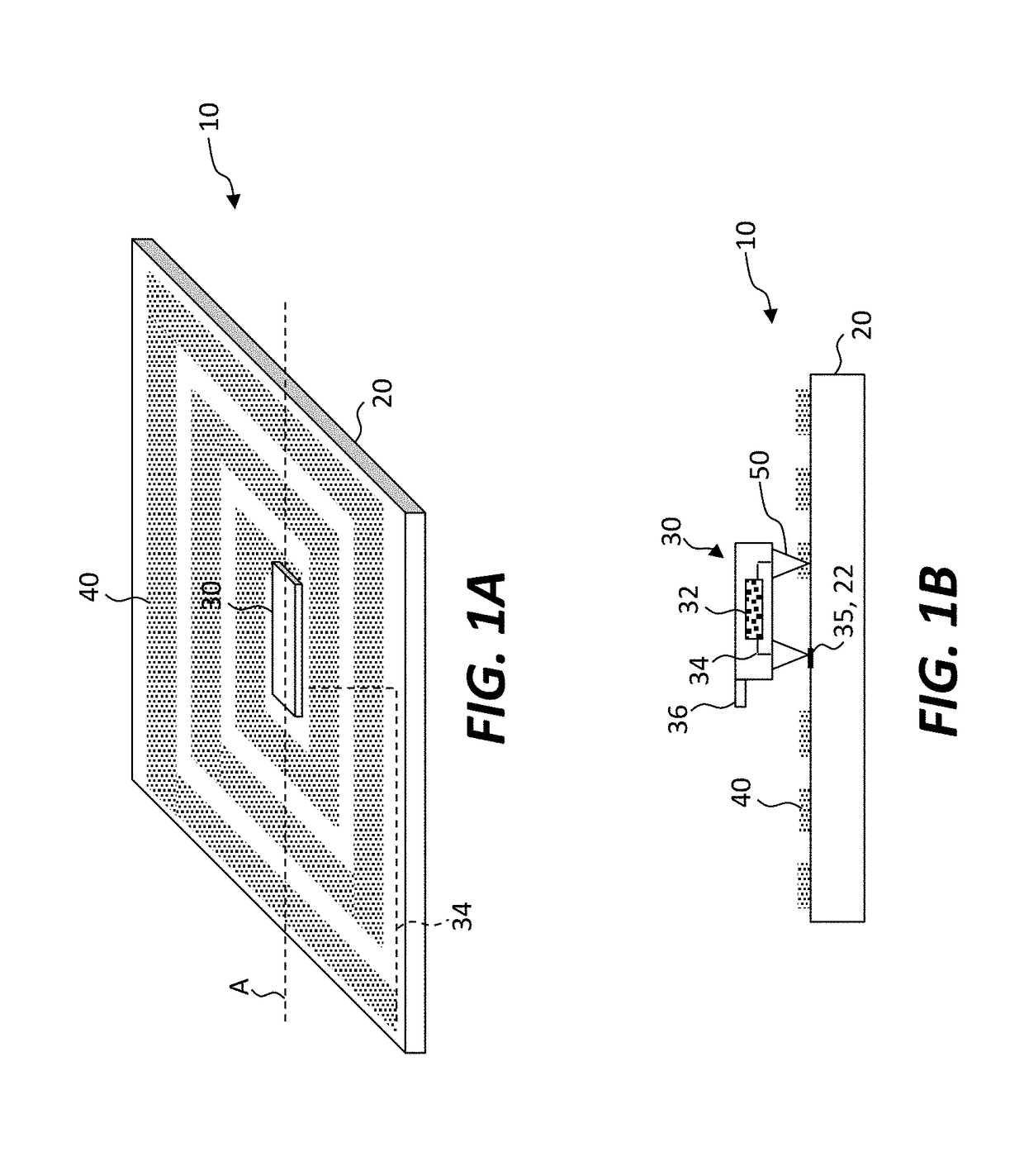
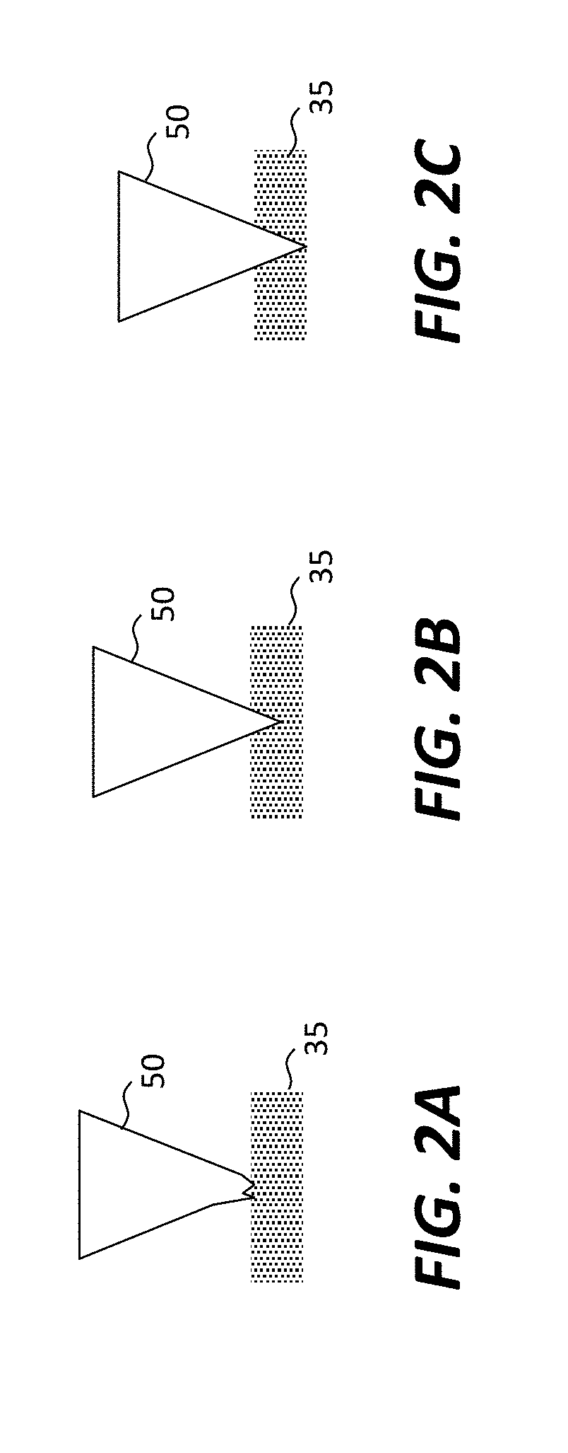
[0055]Referring to the perspective of FIG. 1A and the corresponding cross section of FIG. 1B along cross section line A of FIG. 1A, in some embodiments of the present invention an electromagnetic communication device 10 includes a device substrate 20 and an antenna 40 formed on or in the device substrate 20. A circuit element 30 has an electrical circuit 32 and one or more electrically conductive connection posts 50 protruding from the circuit element 30 or from a surface of the circuit element 30. Each of the connection posts 50 is electrically connected to the electrical circuit 32, for example with a wire 34, and at least one connection post 50 is electrically connected to the antenna 40. The circuit element 30 can be a micro-transfer printed circuit element 30 that includes a fractured tether 36. In some embodiments, the communication device is a radio frequency identification device (RFID) or a near-field communication (NFC) device.

[0056]The device substrate 20 can be any rigid...


PUM


Abstract

An electromagnetic communication device includes a device substrate, an antenna formed on or in the device substrate, and a circuit element having an electrical circuit and one or more electrically conductive connection posts protruding from the circuit element. Each of the connection posts is electrically connected to the electrical circuit and at least one connection post is electrically connected to the antenna.

Description

PRIORITY APPLICATION[0001]This application claims priority to and benefit of U.S. Patent Application No. 62 / 338,265, filed May 18, 2016, entitled Antenna with Micro-Transfer-Printed Circuit Element, the content of which is hereby incorporated by reference in its entirety.CROSS REFERENCE TO RELATED APPLICATION[0002]Reference is made to U.S. Pat. No. 8,889,485, entitled Methods for Surface Attachment of Flipped Active Components by Christopher Bower, the disclosure of which is incorporated herein by reference in its entirety.FIELD OF THE INVENTION[0003]The present invention relates to structures and methods for electrically interconnecting electrical circuit elements to antennas on device substrates using micro-transfer printing.BACKGROUND OF THE INVENTION[0004]Radio-frequency identification (RFID) devices are attached to products or packaging to provide information about the products. RFID devices typically include a device substrate with an antenna and an integrated circuit disposed...

Claims


Application Information

Patent Timeline
IPC IPC(8): H01Q1/22G06K19/077G06K7/10H01Q7/00H01Q1/38
CPCH01Q1/2225H01Q1/2283G06K19/077H01Q1/38H01Q7/00G06K7/10366H01Q9/27G06K19/07775H01L2224/18H01L2224/16227H01L2924/15192H01L2223/6677H01L23/49855
Inventor COK, RONALD S.
Owner X CELEPRINT LIMITED
Why Eureka
Try Eureka