
System and Method for Widening Fin Widths for Small Pitch FinFET Devices

a technology of finfet and wide fins, which is applied in the direction of semiconductor devices, basic electric elements, electrical appliances, etc., can solve the problems of unintended bending or even collapse of the fin, difficult to achieve a wide enough fin width target, and drawbacks of conventional finfet devices

Active Publication Date: 2017-12-28
TAIWAN SEMICON MFG CO LTD
View PDF7 Cites 10 Cited by
  • Summary
  • Abstract
  • Description
  • Claims
  • Application Information

AI Technical Summary

Benefits of technology

The present disclosure offers advantages over conventional FinFET and its fabrication. One advantage is the small fin pitch size while maintaining a sufficient fin width, which leads to less bending and carrier mobility degradation problems and increases device yield and performance. Another advantage is the increased nitrogen content in the dielectric layers surrounding the semiconductor fin structures, which helps ensure the fin structures maintain their integrity and purity. The nitridation processes of the present disclosure are compatible with existing processing steps and easy to implement without increasing costs.

Problems solved by technology

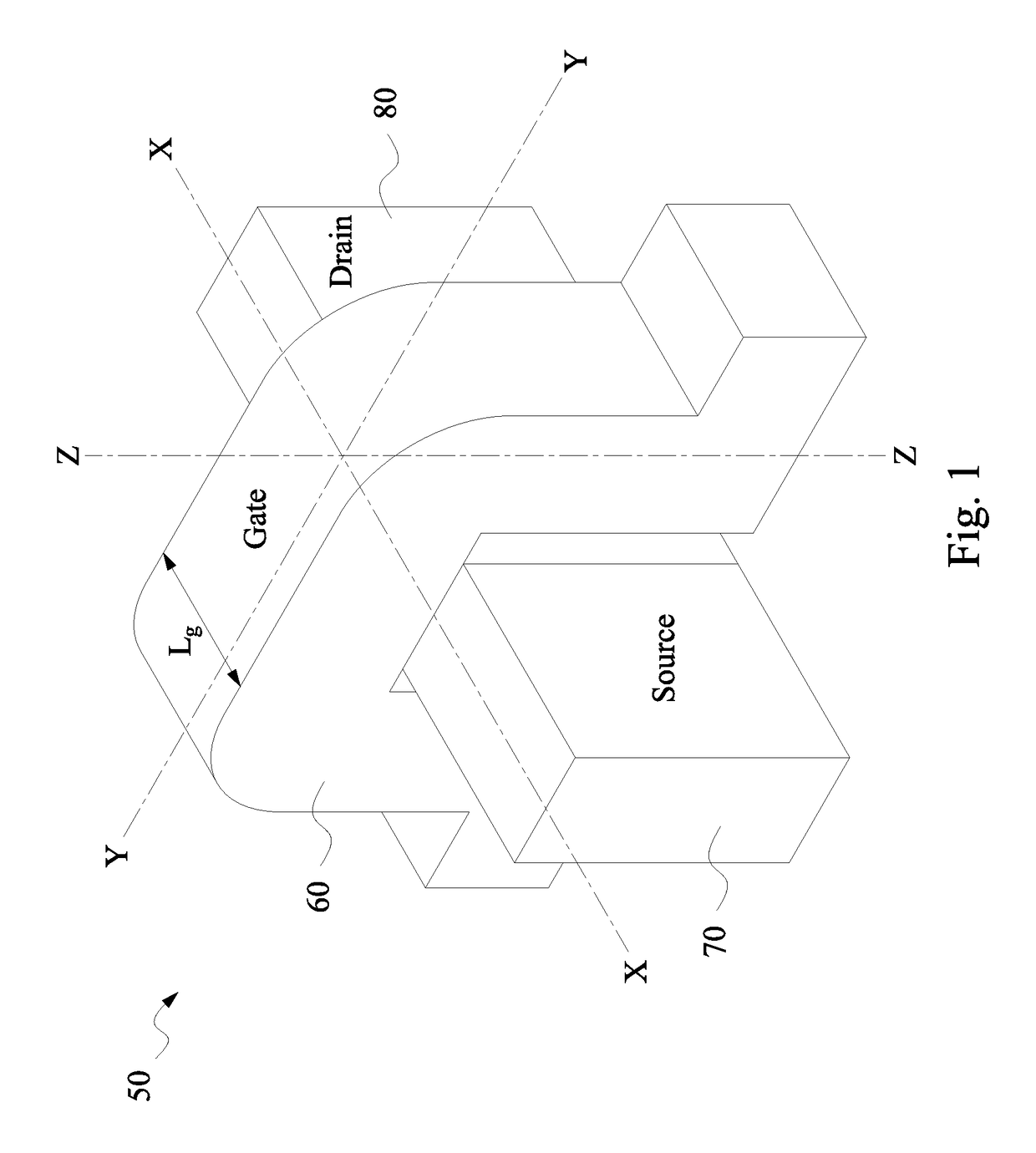
As this progression takes place, challenges from both fabrication and design issues have resulted in the development of three-dimensional designs, such as fin-like field effect transistor (FinFET) device.
However, conventional FinFET devices may still have certain drawbacks.
One drawback is that, as the pitch size continues to shrink, it may be difficult to achieve a fin width target that is wide enough.
Such a small fin width may lead to unintended bending or even collapse of the fin.
The small fin width may also induce carrier mobility degradation.
Consequently, device performance is compromised, or device failure rate may increase.
Therefore, while existing FinFET devices and the fabrication thereof have been generally adequate for their intended purposes, they have not been entirely satisfactory in every aspect.

Method used


Image

  • System and Method for Widening Fin Widths for Small Pitch FinFET Devices
  • System and Method for Widening Fin Widths for Small Pitch FinFET Devices
  • System and Method for Widening Fin Widths for Small Pitch FinFET Devices

Examples


Embodiment Construction

[0010]It is understood that the following disclosure provides many different embodiments, or examples, for implementing different features of the invention. Specific examples of components and arrangements are described below to simplify the present disclosure. These are, of course, merely examples and are not intended to be limiting. For example, the formation of a first feature over or on a second feature in the description that follows may include embodiments in which the first and second features are formed in direct contact, and may also include embodiments in which additional features may be formed between the first and second features, such that the first and second features may not be in direct contact. In addition, the present disclosure may repeat reference numerals and / or letters in the various examples. This repetition is for the sake of simplicity and clarity and does not in itself dictate a relationship between the various embodiments and / or configurations discussed. M...


PUM


Abstract

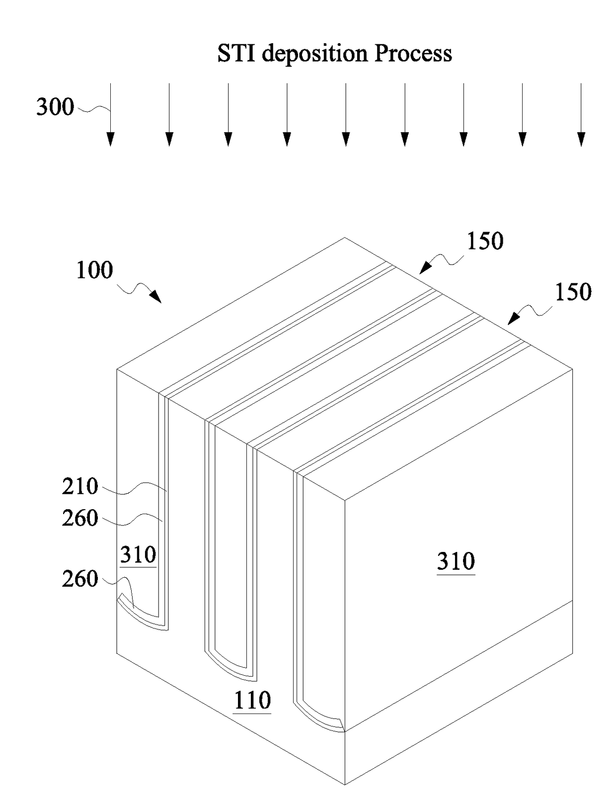
A FinFET includes a semiconductor layer having a fin structure that protrudes out of the semiconductor layer. The fin structure includes a first segment and a second segment disposed over the first segment. A dielectric layer is disposed over the semiconductor layer. The first segment of the fin structure is surrounded by the dielectric layer. A metal layer is disposed over the dielectric layer. The second segment of the fin structure is surrounded by the metal layer. The dielectric layer has a greater nitrogen content than the metal layer. The first segment of the fin structure also has a first side surface that is rougher than a second side surface of the second segment of the fin structure.

Description

PRIORITY DATA[0001]This application claims priority to U.S. Provisional Patent Application Ser. No. 62 / 355,389, filed on Jun. 28, 2016, the entire disclosure of which is hereby incorporated herein by reference.BACKGROUND[0002]The semiconductor industry has progressed into nanometer technology process nodes in pursuit of higher device density, higher performance, and lower costs. As this progression takes place, challenges from both fabrication and design issues have resulted in the development of three-dimensional designs, such as fin-like field effect transistor (FinFET) device. A typical FinFET device is fabricated with a thin “fin” (or fin-like structure) extending from a substrate. The fin usually includes silicon and forms the body of the transistor device. The channel of the transistor is formed in this vertical fin. A gate is provided over (e.g., wrapping around) the fin. This type of gate allows greater control of the channel. Other advantages of FinFET devices include reduc...

Claims


Application Information

Patent Timeline
Patent Type & Authority Applications(United States)
IPC IPC(8): H01L21/8234H01L21/762H01L21/02H01L29/78
CPCH01L21/823431H01L21/0214H01L21/02532H01L21/02592H01L21/02634H01L29/7851H01L21/823481H01L21/02271H01L21/76237H01L21/02164H01L21/02247H01L21/823821H01L29/66545H01L29/66795H01L29/7853
Inventor CHING, KUO-CHENGJU, SHI NINGWANG, CHIH-HAOLEUNG, YING-KEUNGDIAZ, CARLOS H.
Owner TAIWAN SEMICON MFG CO LTD
Learn More