Fabrication of a vertical fin field effect transistor with an asymmetric gate structure

a technology of vertical fin and gate structure, applied in the direction of basic electric elements, electrical apparatus, semiconductor devices, etc., can solve the problems of difficult formation of individual components and electrical contacts, and achieve the effect of reducing the lateral dimensions of sacrificial mandrels

Active Publication Date: 2017-12-28
SAMSUNG ELECTRONICS CO LTD
View PDF2 Cites 268 Cited by
  • Summary
  • Abstract
  • Description
  • Claims
  • Application Information

AI Technical Summary

Benefits of technology

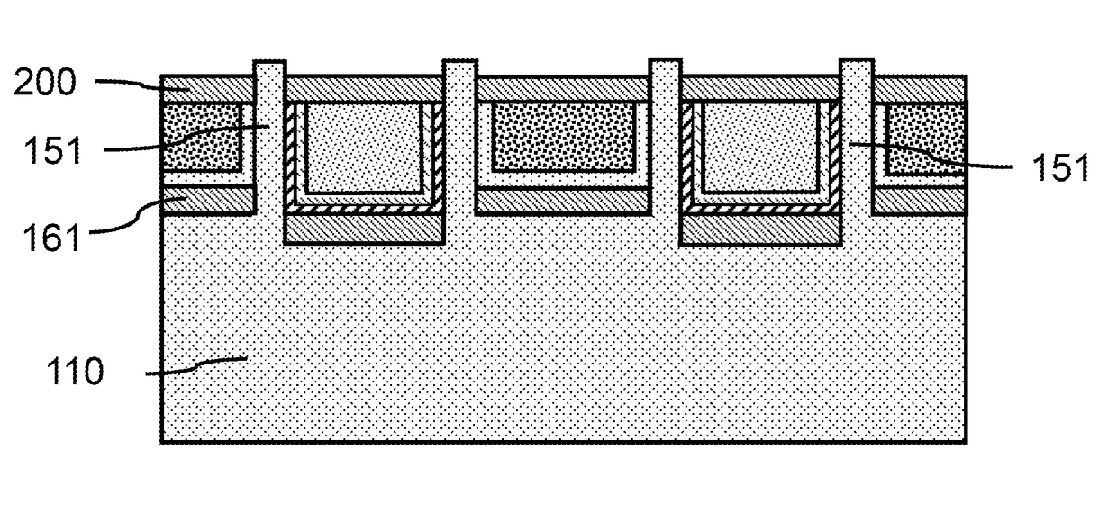
[0005]In accordance with an embodiment of the present principles, a method is provided for forming a vertical fin field effect transistor (vertical finFET) with two concentric gate structures. The method includes the step of forming one or more tubular vertical fins on a substrate, forming a first gate structure around an outer wall of at least one of the one or more tubular vertical fins, and forming a second gate structure within an inner wall of at least one of the one or more tubular vertical fins having the first gate structure around the outer wall.
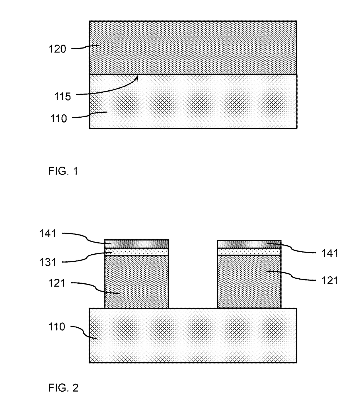
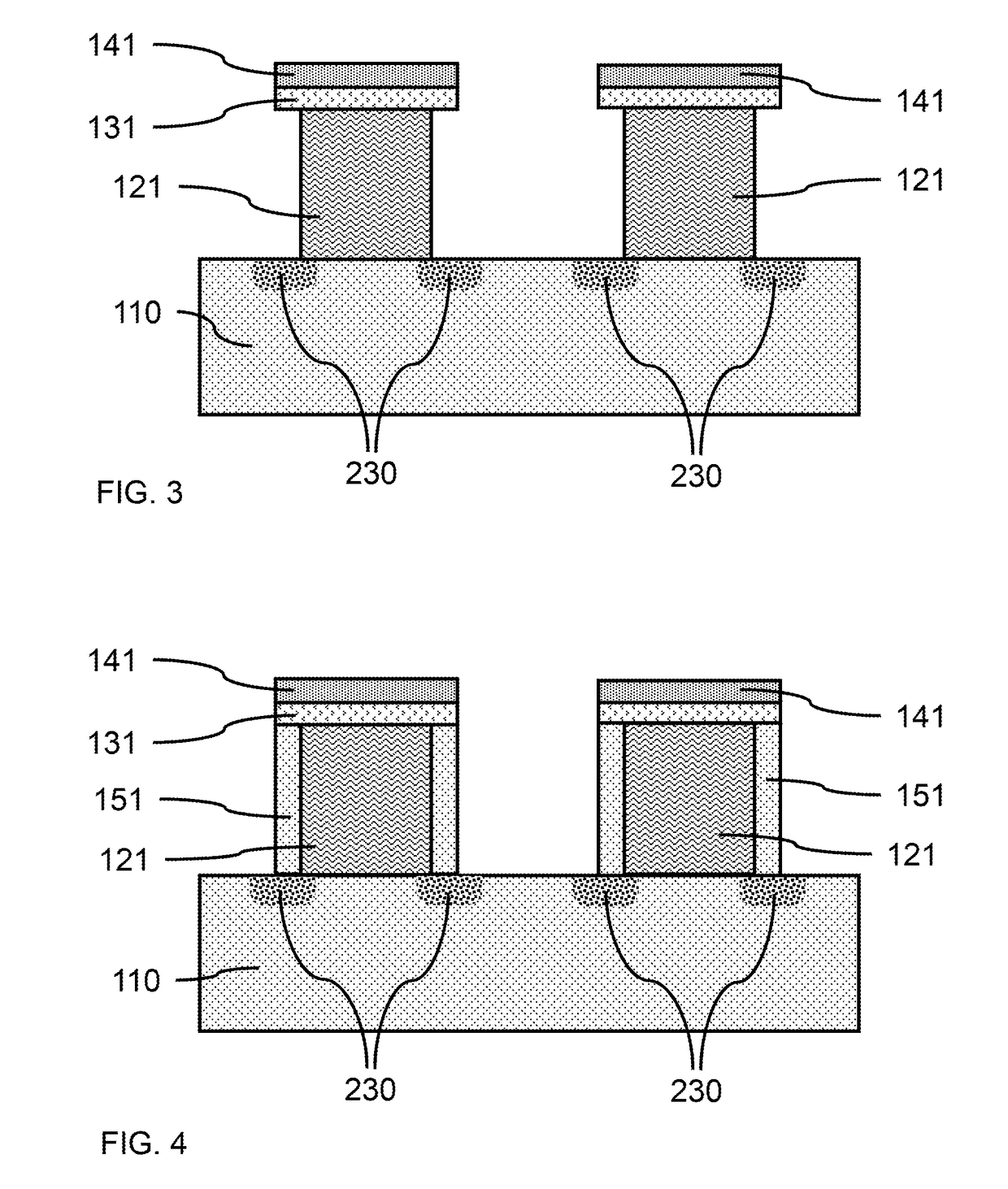
[0006]In accordance with an embodiment of the present principles, a method is provided for forming a vertical fin field effect transistor (vertical finFET) with two concentric gate structures. The method includes the step of forming a plurality of sacrificial mandrels on a substrate and reducing the lateral dimensions of the sacrificial mandrels. The method further includes the step of forming a tubular vertical fin on each of the plurality of sacrificial mandrels. The method further includes the step of forming a first gate structure around an outer wall of at least one of the plurality tubular vertical fins, removing the plurality of sacrificial mandrels, and forming a second gate structure on at least a portion of an inner wall of each tubular vertical fin.
[0007]In accordance with another embodiment of the present principles, a vertical fin field effect transistor device with a concentric gate structure is provided. The device includes a tubular vertical fin, a first gate structure formed on at least a portion of the outer wall of the tubular vertical fin, and a second gate structure formed on at least a portion of the inner wall of the tubular vertical fin.

Problems solved by technology

With ever decreasing device dimensions, forming the individual components and electrical contacts become more difficult.

Method used


Image

  • Fabrication of a vertical fin field effect transistor with an asymmetric gate structure
  • Fabrication of a vertical fin field effect transistor with an asymmetric gate structure
  • Fabrication of a vertical fin field effect transistor with an asymmetric gate structure

Examples


Embodiment Construction

[0039]Principles and embodiments of the present disclosure relate generally to fabricating two separate gate structures on the same vertical fin to affect broader control of current in the vertical channel of a finFET. A first gate may be configured and used for current control in the channel, while the second gate may be configured and used as a back gate to apply a voltage bias to adjust a threshold voltage of the finFET. In various embodiments, the two separate gate structures may operate independently, where each gate structure may have a separate electrical contact. In various embodiments, the two separate gate structures may be formed on the vertical fins without greatly increasing the complexity of the fabrication process.

[0040]Principles and embodiments of the present disclosure relate generally to avoiding formation of a wrap-around gate on a vertical fin by arranging the two gates and the channel concentrically, where a first gate is surrounded by a wall of the fin materia...


PUM


Abstract

A method of forming a vertical fin field effect transistor (vertical finFET) with two concentric gate structures, including forming one or more tubular vertical fins on a substrate, forming a first gate structure around an outer wall of at least one of the one or more tubular vertical fins, and forming a second gate structure within an inner wall of at least one of the one or more tubular vertical fins having the first gate structure around the outer wall.

Description

BACKGROUNDTechnical Field[0001]The present invention generally relates to a vertical fin field effect transistor structure with two separate gates, and more particularly to a vertical fin field effect transistor (vertical finFET) with a channel control gate and a back gate.Description of the Related Art[0002]A Field Effect Transistor (FET) typically has a source, a channel, and a drain, where current flows from the source to the drain, and a gate that controls the flow of current through the channel. Field Effect Transistors (FETs) can have a variety of different structures, for example, FETs have been fabricated with the source, channel, and drain formed in the substrate material itself, where the current flows horizontally (i.e., in the plane of the substrate), and finFETs have been formed with the channel extending outward from the substrate, but where the current also flows horizontally from a source to a drain. A vertical finFET can also be configured with a bottom source / drain...

Claims


Application Information

Patent Timeline
Patent Type & Authority Applications(United States)
IPC IPC(8): H01L29/78H01L21/28H01L29/49H01L29/10H01L29/08H01L29/66H01L29/423
CPCH01L29/7827H01L29/66666H01L29/1037H01L21/28079H01L29/0847H01L29/42376H01L29/66484H01L29/7831H01L29/495H01L29/4966H01L29/517H01L29/66545
Inventor MOCHIZUKI, SHOGOWANG, JUNLI
Owner SAMSUNG ELECTRONICS CO LTD
Why Eureka
Try Eureka