Apparatus and method for polishing a surface of a substrate

a technology of substrate and surface, applied in the direction of grinding machine components, manufacturing tools, lapping machines, etc., can solve the problems of excessive polishing and/or insufficient polishing of the outermost area of the wafer, the number of polishing steps can be reduced, and the consumption of polishing tools is excessiv

Active Publication Date: 2018-01-18
EBARA CORP
View PDF9 Cites 3 Cited by
  • Summary
  • Abstract
  • Description
  • Claims
  • Application Information

AI Technical Summary

Benefits of technology

[0033]According to the above-described embodiments, when the polishing head is polishing the first surface of the substrate, the rollers, gripping the periphery of the substrate, rotate about their respective own axes. Therefore, there is no need to revolve the rollers around the center of the substrate along with the rotation of the substrate. Accordingly, the rollers do not contact the polishing head, and the polishing tool can polish the entirety of the first surface, including an outermost area thereof, of the substrate. As a result, there is no need to polish the outermost area of the surface of the substrate with use of an edge polishing apparatus, and hence the number of polishing steps can be reduced.
[0034]According to the above-described embodiments, the first surface of the substrate can be polished while measuring the amount of foreign matter removed. Therefore, the polishing of the substrate can be terminated when the amount of foreign matter removed reaches a low level. This makes it possible to finish a plurality of substrates, having different initial amounts of foreign matter, into a uniform surface state. Furthermore, the above-described reference examples can prevent a decrease in the throughput, an excessive consumption of the polishing tool, an increase in polishing marks on a substrate, worsening of the polishing profile, etc. due to excessive polishing. A decrease in the yield due to insufficient polishing can also be prevented.

Problems solved by technology

Foreign matter adhering to a device can cause a short-circuit between interconnects or can cause a circuit failure.
As a result, the outermost area of the wafer surface cannot be polished, and needs to be polished separately by using an edge polishing apparatus.
Therefore, constant-time polishing of wafers can cause excessive polishing and / or insufficient polishing of the wafers.

Method used


Image

  • Apparatus and method for polishing a surface of a substrate
  • Apparatus and method for polishing a surface of a substrate
  • Apparatus and method for polishing a surface of a substrate

Examples


Embodiment Construction

[0044]Embodiments will now be described with reference to the drawings.

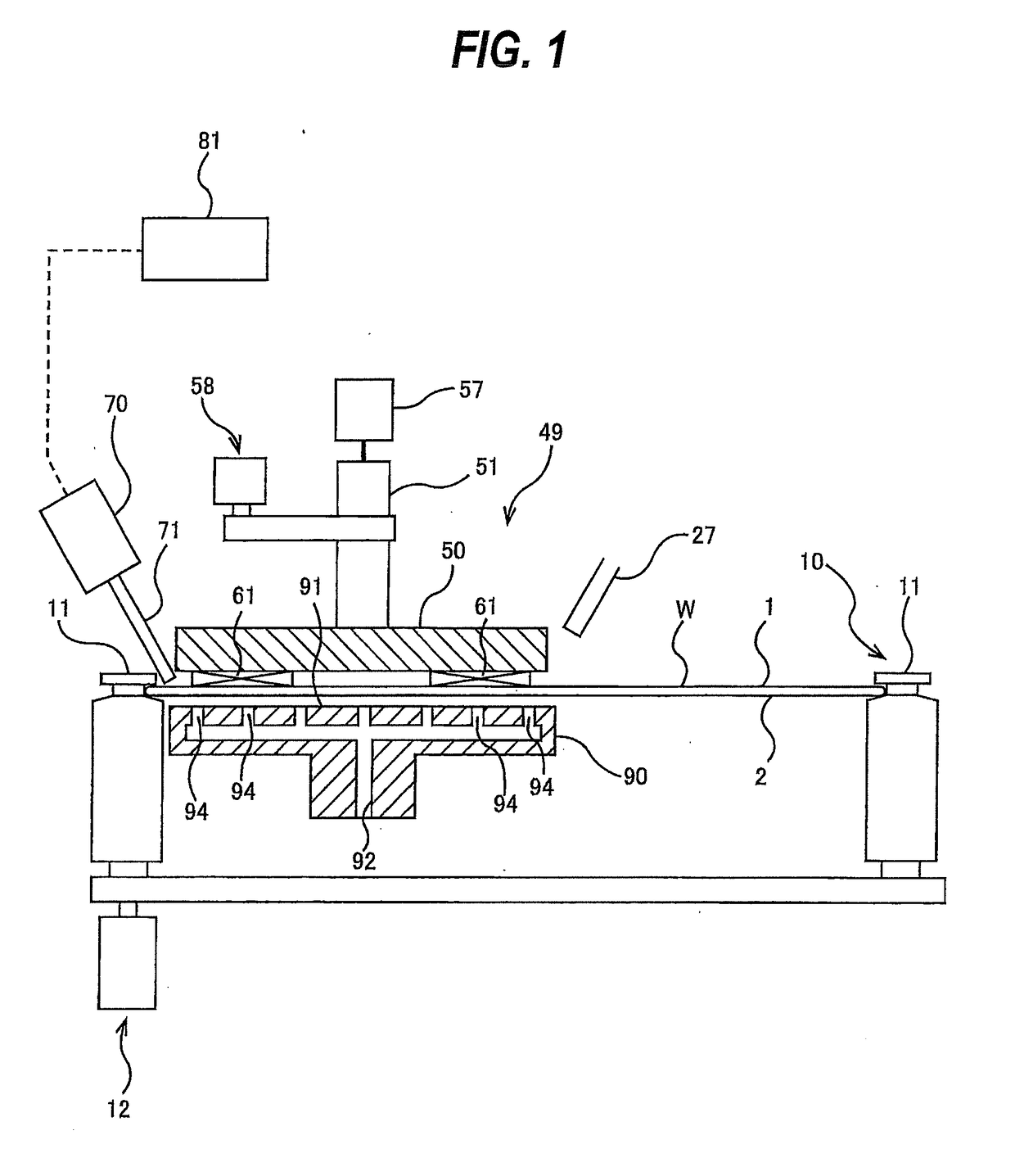
[0045]FIG. 1 is a schematic view showing an embodiment of a polishing apparatus. The polishing apparatus includes a substrate holder 10 for holding a wafer W, which is an example of a substrate, and rotating the wafer W about its axis, a polishing head assembly 49 for polishing a first surface 1 of the wafer W, held by the substrate holder 10, to remove foreign matter, scratches, etc. from the first surface 1 of the wafer W, and a hydrostatic support stage 90 as a substrate support stage for supporting a second surface 2 of the wafer W which is opposite from the first surface 1. The polishing head assembly 49 is disposed above the wafer W held by the substrate holder 10, while the hydrostatic support stage 90 is disposed below the wafer W held by the substrate holder 10.

[0046]In one embodiment, the first surface 1 of the wafer W is a back surface of the wafer W with no device formed thereon, i.e., a non-device su...


PUM


Abstract

An apparatus which can polish an entirety of a surface of a substrate, such as a wafer, is disclosed. The apparatus includes a substrate holder configured to hold a substrate and rotate the substrate; and a polishing head configured to rub a polishing tool against a first surface of the substrate to polish the first surface. The substrate holder includes a plurality of rollers which can contact a periphery of the substrate. The plurality of rollers are rotatable about their respective own axes.

Description

CROSS REFERENCE TO RELATED APPLICATIONS[0001]This document claims priorities to Japanese Patent Application No. 2016-139777 filed Jul. 14, 2016 and Japanese Patent Application No. 2017-051673 filed Mar. 16, 2017, the entire contents of which are hereby incorporated by reference.Background[0002]Devices, such as memory circuits, logic circuits and image sensors (e.g. CMOS sensors) are becoming more highly integrated these days. In a process for forming such devices, foreign matter such as fine particles and dust may ad here to the devices. Foreign matter adhering to a device can cause a short-circuit between interconnects or can cause a circuit failure. Therefore, in order to enhance the reliability of the device, it is necessary to clean a wafer on which the device is formed to remove the foreign matter on the wafer.[0003]The above-described foreign matter, such as fine particles and dust, can may adhere also to a back surface (or a non-device surface) of a wafer. If such foreign mat...

Claims


Application Information

Patent Timeline
Patent Type & Authority Applications(United States)
IPC IPC(8): B08B1/04H01L21/304H01L21/67H01L21/687
CPCB08B1/04H01L21/68728H01L21/67051H01L21/304B24B7/228B24B27/033B24B37/013B24B37/042B24B37/10B24B37/107B24B37/30B24B41/067B24B49/08B24D7/06B24B37/04B24B57/02H01L21/30625H01L21/6875
Inventor ISHII, YUNAKANISHI, MASAYUKIUCHIYAMA, KEISUKE
Owner EBARA CORP
Why Eureka
Try Eureka