Transfer chamber

a technology of transfer chamber and transfer chamber, which is applied in the field of transfer chamber, can solve the problems of increasing the influence of moisture content, oxygen, chemical components, etc., on the structure of semiconductor devices, and achieve the effect of shortening or eliminating the stop time of the transfer process

Active Publication Date: 2018-02-08
SINFONIA TECHNOLOGY CO LTD
View PDF3 Cites 22 Cited by
  • Summary
  • Abstract
  • Description
  • Claims
  • Application Information

AI Technical Summary

Benefits of technology

[0022]According to the present invention described above, it is possible to provide a transfer chamber capable of replacing a gas processing device without affecting an

Problems solved by technology

Further, as the semiconductor device structure decreases in size recently, influences caused by the moisture content, ox

Method used


Image

  • Transfer chamber
  • Transfer chamber
  • Transfer chamber

Examples


Embodiment Construction

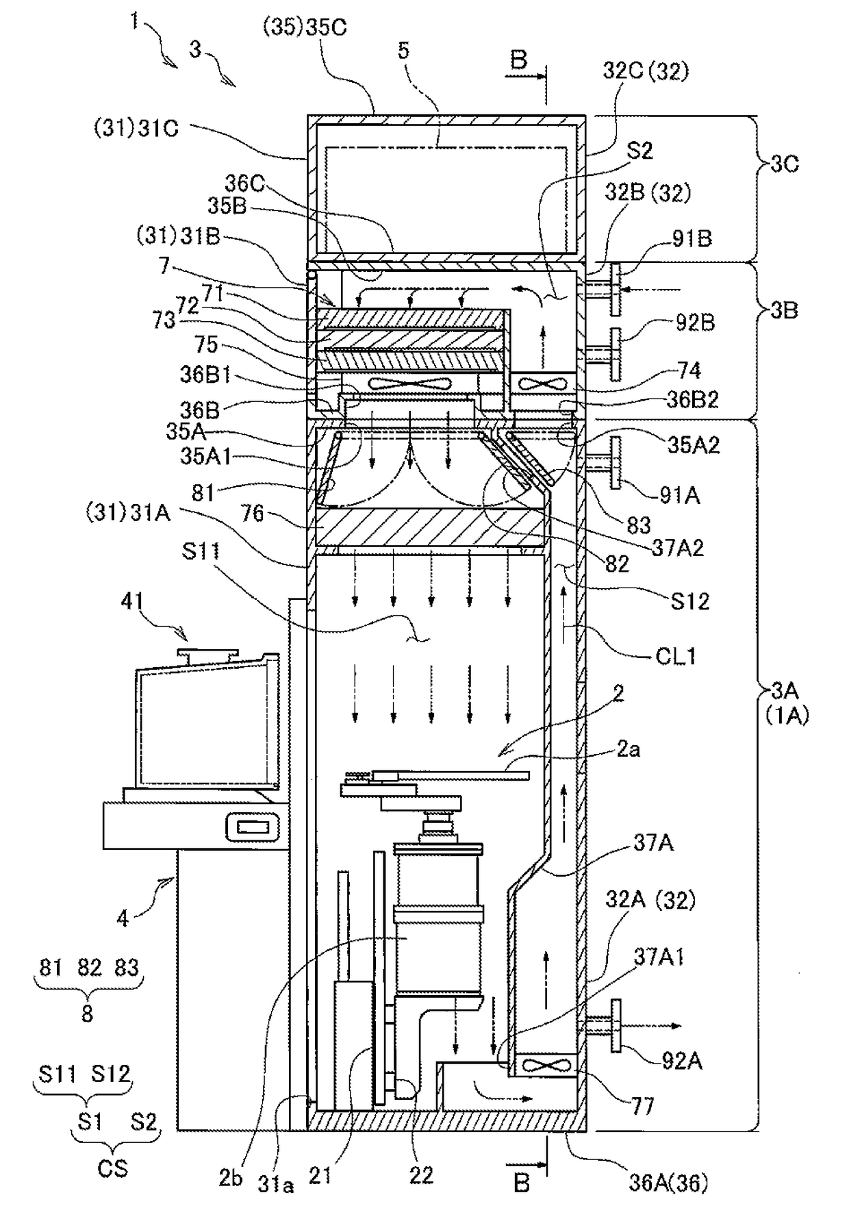
[0032]Hereinafter, an embodiment of the present invention will be described with reference to the drawings.

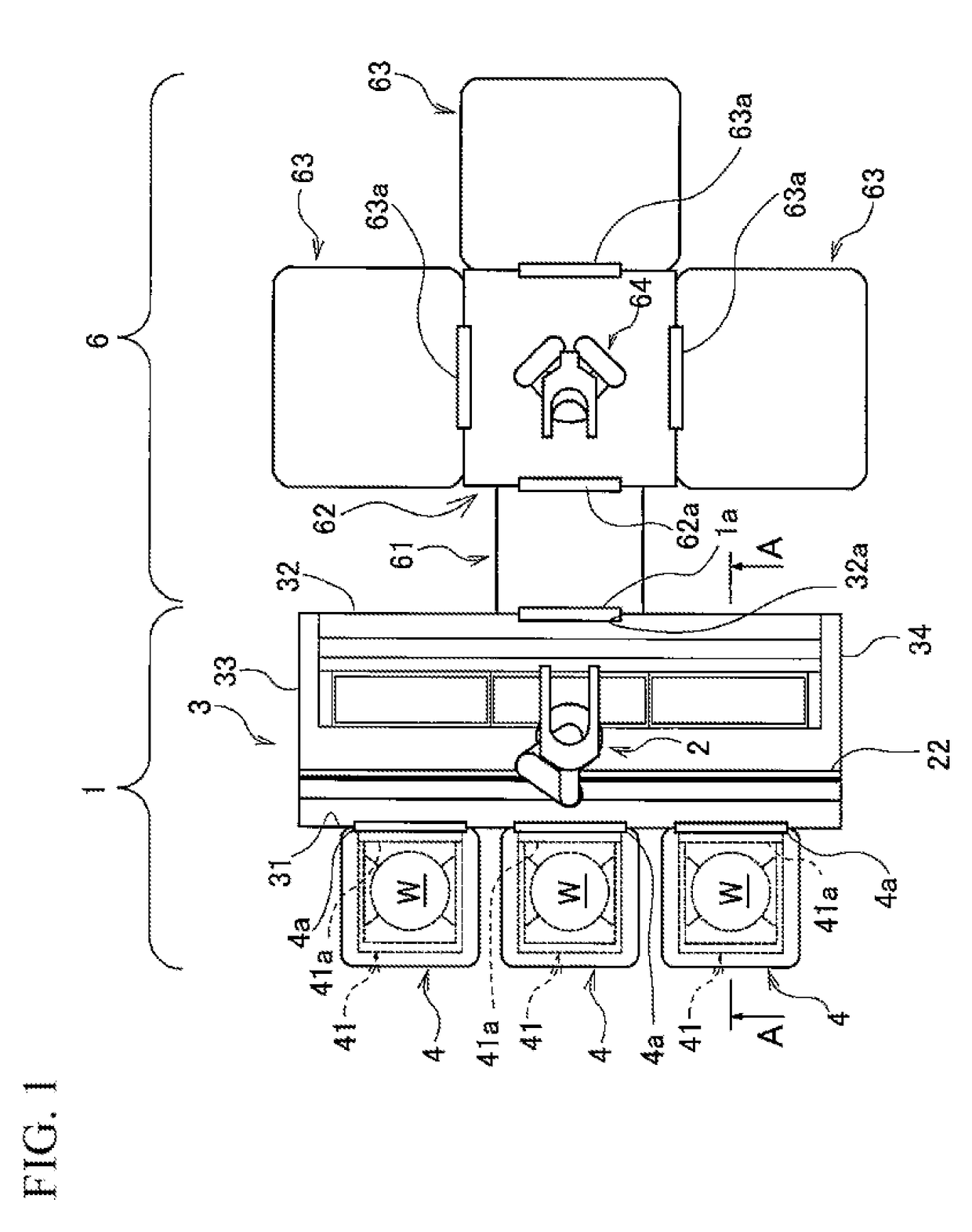
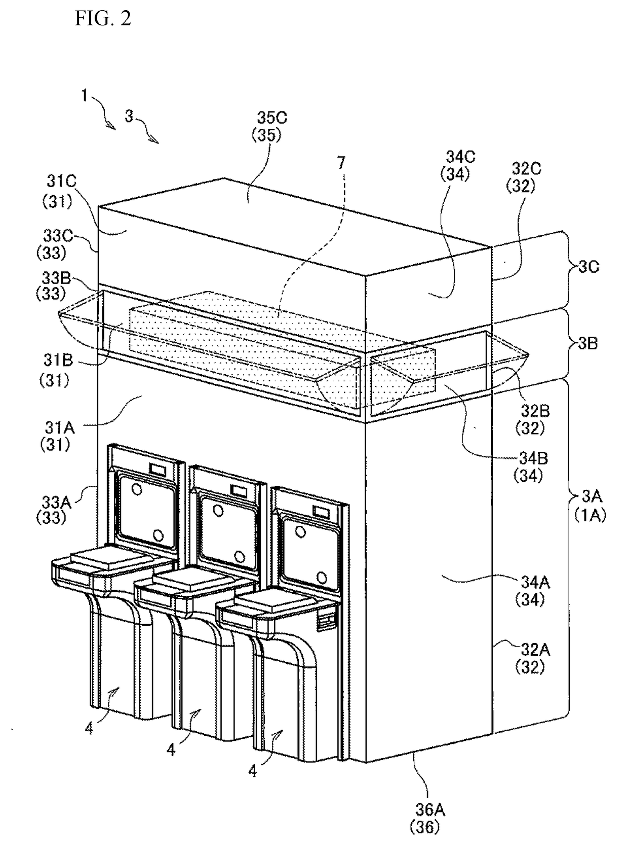
[0033]FIG. 1 is a plan view schematically illustrating a relationship between a transfer chamber 1 according to an embodiment of the present invention and a processing device 6 connected to the transfer chamber 1. As illustrated in FIG. 1, the transfer chamber 1 is constituted as module equipment generally referred to as an EFEM. In particular, the transfer chamber 1 includes a transfer robot 2 which transfers a wafer W which is a transferred object between prescribed transfer positions, a box-shaped housing 3 provided to surround the transfer robot 2, and a plurality of (three in FIG. 1) load ports 4 connected to the outside of a wall on the front side of the housing 3 (a front wall 31).

[0034]Here, in the present application, the direction in which the load ports 4 are connected when seen from the housing 3 is defined as the front side, the direction of a rear wall 32 opposite...


PUM


Abstract

To provide a transfer chamber capable of replacing a chemical filter without affecting an internal atmosphere, and shortening or eliminating stop time of a transfer process of a wafer (W) associated with replacement of the chemical filter. The transfer chamber transfers the wafer (W) to or from a processing device (6) by using a transfer robot (2) provided thereinside, and includes a circulation path (CL1) formed inside of a transfer chamber (1) to circulate gas, a chemical filter unit (7) provided in the midstream of the circulation path (CL1), and a connecting and disconnecting means (8) which switches connection and disconnection of the chemical filter unit (7) to and from the circulation path (CL1).

Description

TECHNICAL FIELD[0001]The present invention relates to a transfer chamber capable of transferring a transferred object in a clean state without exposing to the outside air.BACKGROUND ART[0002]In the field of semiconductor, a semiconductor device is conventionally manufactured by applying various processing steps to a wafer.[0003]In the semiconductor device manufacturing process, a particle-less and chemical component-less transfer environment of a wafer has been required, and a closed type container called an FOUP (Front-Opening Unified Pod) and a transfer chamber generally called an EFEM (Equipment Front End Module) which transfers a wafer to or from a processing device are used (see the following Patent Literature 1). In the transfer chamber, usually, fresh outside air in a clean room is taken into an FFU (Fun Filter Unit) installed in an upper part, and the air is made to flow downward inside of the transfer chamber and exhausted to the outside from a floor surface, so as to stabl...

Claims


Application Information

Patent Timeline
IPC IPC(8): H01L21/67B01D53/42C12M1/12F24F13/28F24F6/00H01L21/687B01D53/40F24F7/06F24F7/003
CPCH01L21/67196B01D53/40B01D53/42F24F7/06F24F13/28F24F6/00H01L21/68707C12M37/00B01D2258/02B01D53/04B65G49/07H01L21/67017H01L21/67766F24F7/003F24F3/167F24F7/065F24F7/08H01L21/67389H01L21/67393
Inventor KAWAI, TOSHIHIROSHIGETA, TAKASHIKOMIYA, MUNEKAZUTANIYAMA, YASUSHI
Owner SINFONIA TECHNOLOGY CO LTD
Why Eureka
Try Eureka