Defect inspection method and defect inspection apparatus

a technology of defect inspection and inspection method, applied in the direction of material analysis using wave/particle radiation, instruments, image enhancement, etc., can solve the problem that the detection signal of a defect of interest may be relatively weak

a technology of defect inspection and inspection method, applied in the direction of material analysis using wave/particle radiation, instruments, image enhancement, etc., can solve the problem that the detection signal of a defect of interest may be relatively weak

US20180053295A1Active Publication Date: 2018-02-22SAMSUNG ELECTRONICS CO LTD

Image

  • Defect inspection method and defect inspection apparatus
  • Defect inspection method and defect inspection apparatus
  • Defect inspection method and defect inspection apparatus

Examples


Embodiment Construction

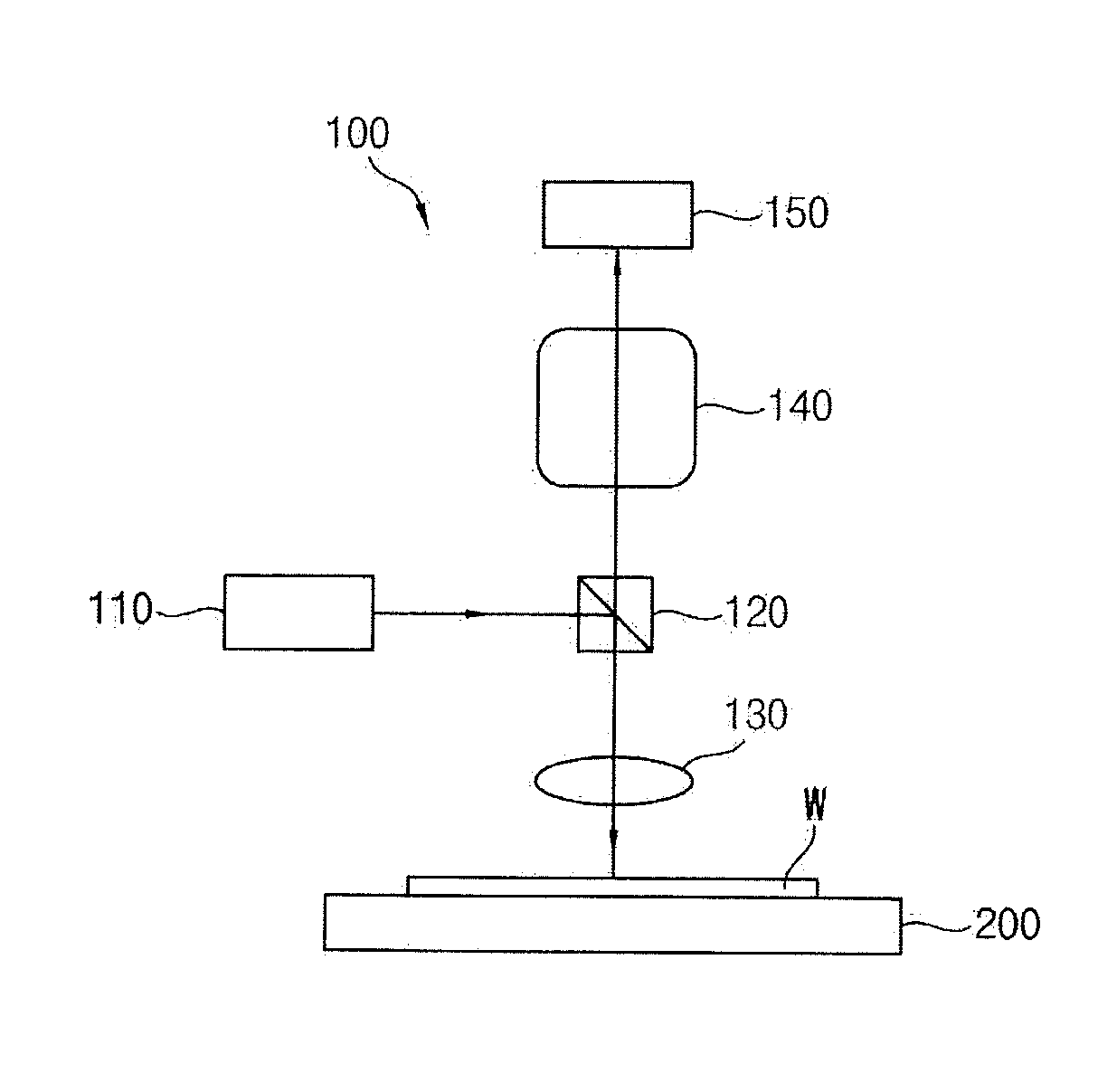
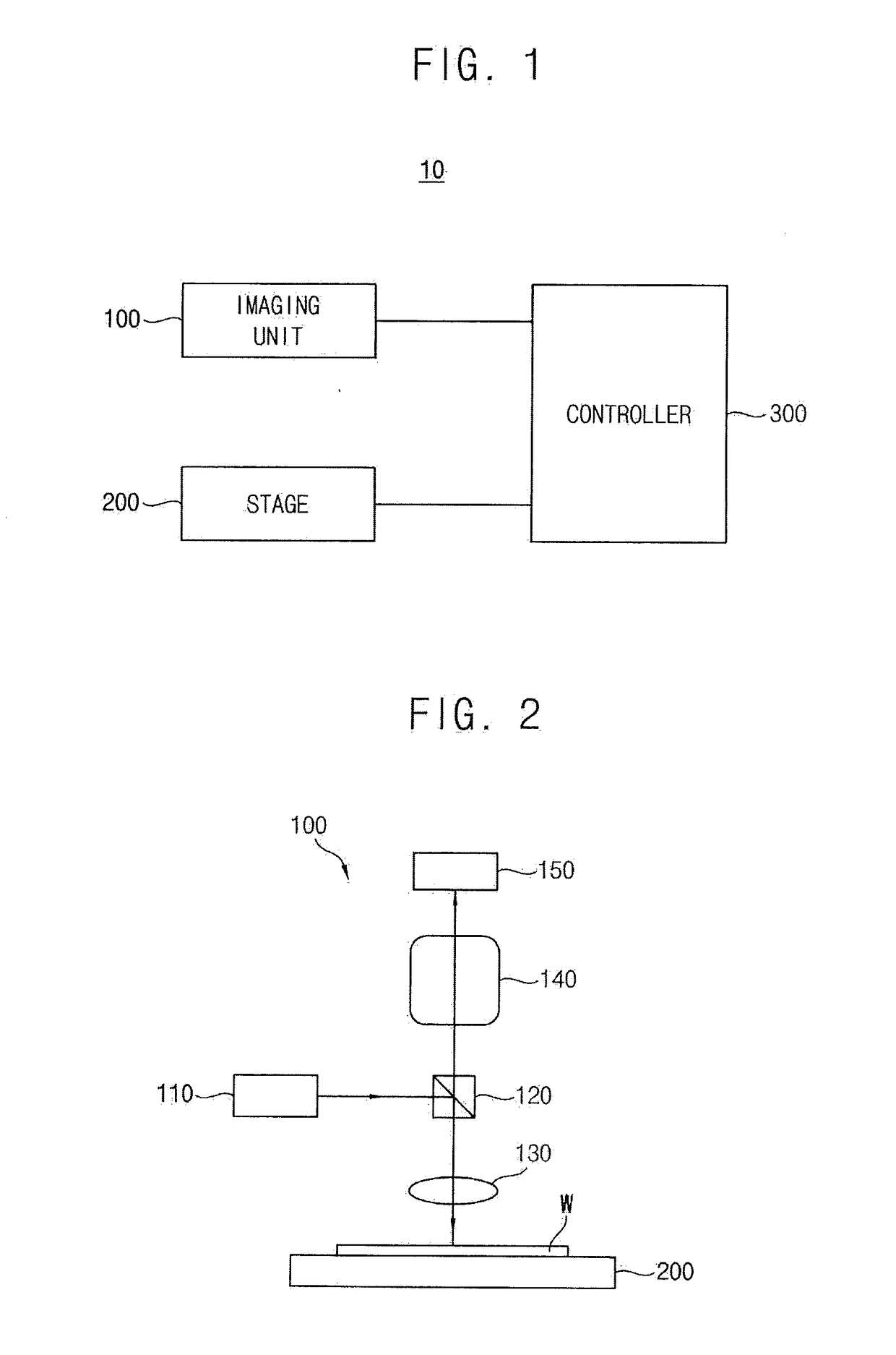
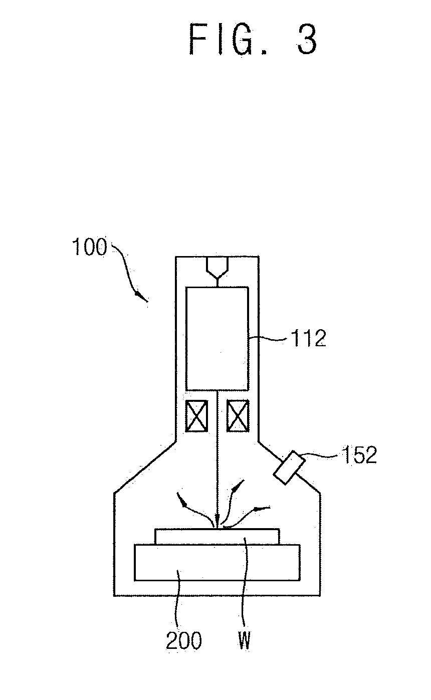
[0022]FIG. 1 is a view illustrating a defect inspection apparatus in accordance with example embodiments of the present inventive concepts. FIG. 2 is a cross-sectional view illustrating an imaging unit of a defect inspection apparatus in accordance with some example embodiments of the present inventive concepts. FIG. 3 is a cross-sectional view illustrating an imaging unit of a defect inspection apparatus in accordance with other example embodiments of the present inventive concepts. FIG. 4 is a block diagram illustrating a controller of the defect inspection apparatus in FIG. 1 in accordance with example embodiments of the present inventive concepts. FIG. 5 is a view illustrating multiple scanning of the defect inspection apparatus in FIG. 1 in accordance with example embodiments of the present inventive concepts.

[0023]Referring to FIGS. 1 to 5, a defect inspection apparatus 10 may include an imaging unit 100, a stage 200 and a controller 300.

[0024]In example embodiments, the defec...


PUM


Abstract

In a defect inspection method, first and second inspection conditions having a first sensitivity of detection signal and having a second sensitivity of a detection signal for a defect of interest (DOI), respectively, are determined. The first and second sensitivities are different. First and second images of the same detection region on a substrate surface under the first and second inspection conditions respectively, are obtained. The first and second images are matched to detect a defect in the detection region.

Description

PRIORITY STATEMENT[0001]This application claims priority under 35 U.S.C. §119 to Korean Patent Application No. 10-2016-0104096, filed on Aug. 17, 2016 in the Korean Intellectual Property Office (KIPO), the contents of which are herein incorporated by reference in their entirety.BACKGROUND1. Field[0002]Example embodiments relate to a defect inspection method and a defect inspection apparatus. More particularly, example embodiments relate to a defect inspection method for detecting a defect of a pattern formed on a wafer. Example embodiments further relate to a defect inspection apparatus for performing the same.2. Description of the Related Art[0003]In semiconductor manufacturing, optical metrology is typically employed for measuring and evaluating properties such as optical properties, shapes of nano patterns, and the like, of nano samples. In particular, nano-samples can be measured and evaluated in real time in a non-destructive manner, for example, in a non-contact manner. In a c...

Claims


Application Information

Patent Timeline
22 Feb 2018
Publication
US20180053295A1
IPC
G06T7/00; G06T7/11; G06T7/174; G02B21/00; G01N23/225; G01N21/956; G01N21/95; H01J37/22
CPC
G06T7/0004; G06T7/11; G06T7/174; G02B21/0036; G02B21/008; G01N23/2251; H01J2237/24578; G01N21/9501
Inventors
RYU, SUNG-YOON; SONG, JOON-SEO