
Ultra-low-voltage CMOS circuit and the same for memory

Active Publication Date: 2018-03-01
ETRON TECH INC
View PDF1 Cites 17 Cited by
  • Summary
  • Abstract
  • Description
  • Claims
  • Application Information

AI Technical Summary

Benefits of technology

The present invention allows for the development of logic circuits for SoCs (System-on-Chips) and SRAMs (Simple Random Access Memory) that operate at low voltage, low power, and high speed. Additionally, it reduces the number of power-supply voltages needed for the SRAM, which can benefit the performance of peripheral circuits that may also use boosted power supply voltages for 5T SRAM cells.

Problems solved by technology

Third, other arising issues, for example, desirable voltage relationships between memory cells and peripheral circuits, how to ensure operations over wide range of VDD under VDH and VSL, and how to balance “1” read speed with “0” read speed.

Method used


Image

  • Ultra-low-voltage CMOS circuit and the same for memory
  • Ultra-low-voltage CMOS circuit and the same for memory
  • Ultra-low-voltage CMOS circuit and the same for memory

Examples


Embodiment Construction

[0051]For a circuit 600 with a large output capacitance Cout to operate at low power and high speed, there is a concept of applications of BPS and GS-DD, as shown in FIG. 6. The circuit 600 is composed of a receiver REC, a BPS-booster BST, and an output buffer BF. The receiver REC can include a low-Vt (e.g., ZVT) circuit to receive a small voltage (0.3V) swing input IN. The booster BST includes a conventional high-Vt logic circuit operating at boosted voltages (VDH and −VSL). The output buffer BF includes a low-Vt (e.g., ZVT) inverter. At least the receiver REC and the booster BST are controlled by a shifter SFT. This concept is very effective for low power of long and large number of interconnect lines such as address lines and data-in and data-out lines. Note that if VDH and / or −VSL used in peripheral circuits are set to be same as those in 5T memory cells, a number of power supplies as the while SRAM are reduced, enabling low-cost and simple design. The details are explained lat...


PUM


Abstract

A memory includes a plurality of memory cells and a plurality of peripheral circuits. Each memory cell has a first inverter and a second inverter, the first inverter is supplied by a first power supply rail and a second power supply rail, and the second inverter is supplied by a third power supply rail and a fourth power supply rail. A first voltage difference is applied across the first power supply rail and the second power supply rail, a second voltage difference is applied across the third power supply rail and the fourth power supply rail, and the first voltage difference is less than the second voltage difference. The plurality of peripheral circuits use at least one of boosted power supplies corresponding to the second voltage difference and gate-source differentially-driven circuits.

Description

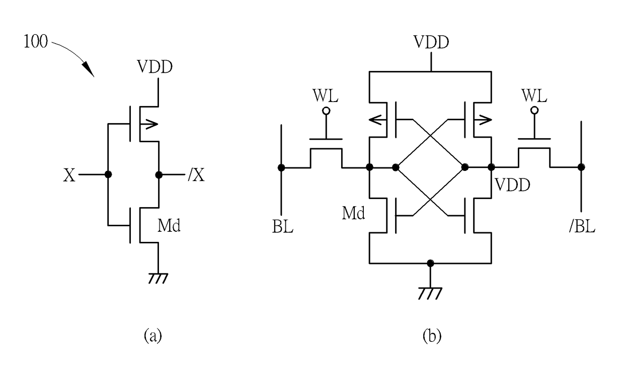
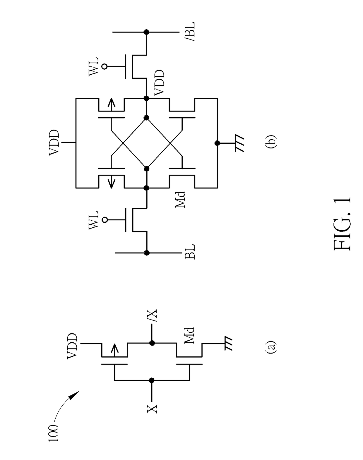
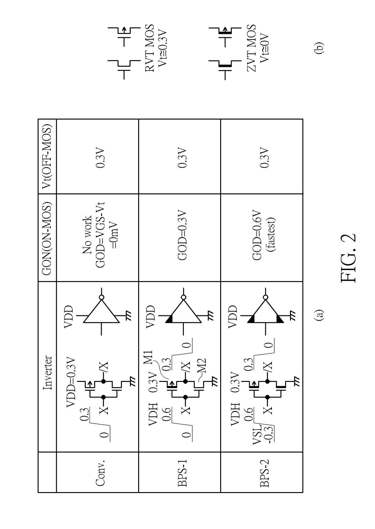
CROSS REFERENCE TO RELATED APPLICATIONS[0001]This application claims the benefit of U.S. Provisional Application No. 62 / 378,692, filed on Aug. 24, 2016 and entitled “Ultra-Low-Voltage CMOS Circuits and Applications to SRAMs,” the contents of which are incorporated herein by reference.BACKGROUND OF THE INVENTION1. Field of the Invention[0002]The present invention relates to a static random access memory, particularly to a static random access memory (SRAM), in which basic logic circuits never operate at low voltage at less than 0.5V (namely sub-0.5V) with low power and high speed.2. Description of the Prior Art[0003]FIG. 1(a) depicts a basic CMOS (complementary metal-oxide-semiconductor) inverter 100, wherein gate-over-drive (GOD) of a MOS is defined as subtraction of a threshold voltage Vt of the MOS from a gate-source voltage VGS (i.e., GOD=VGS−Vt) of the MOS. For example, as shown in FIG. 1(a), when an input X of the CMOS inverter 100 changes from 0V to a supply voltage VDD, GOD(M...

Claims


Application Information

Patent Timeline
Patent Type & Authority Applications(United States)
IPC IPC(8): G11C11/417
CPCG11C11/417G11C13/0007
Inventor ITOH, KIYOO
Owner ETRON TECH INC
Learn More