

Watermarked paper
- Summary
- Abstract
- Description
- Claims
- Application Information
AI Technical Summary
Benefits of technology
Problems solved by technology
Method used
Image

Examples
first embodiment
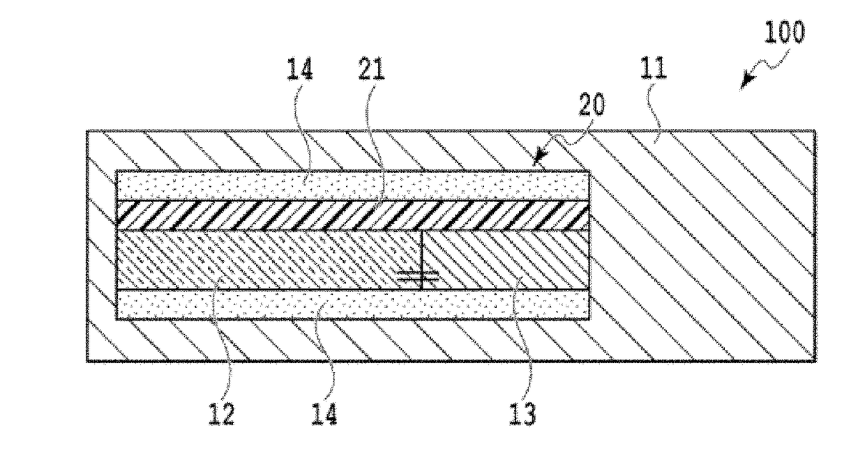
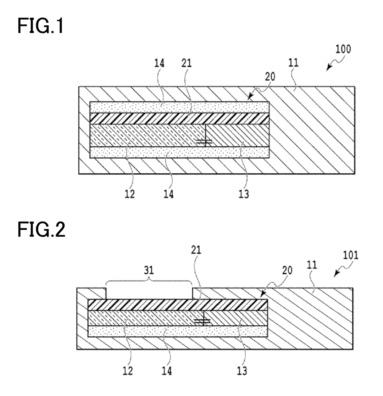
[0032]FIG. 1 is a cross-sectional view showing a layer configuration of watermarked paper according to the first embodiment. In the watermarked paper 100, an intermediate layer 20 having a dimmer 12 and a power supply 13 is mixed into a paper base material 11. The intermediate layer 20 has at least the dimmer 12, and may have optionally transparent layers such as an adhesive layer 14 and an intermediate layer base material 21 as long as they do not prevent transmission of light. The power supply 13 may be provided in the intermediate layer 20 as shown in FIG. 1, but also can be provided on the surface of the watermarked paper 100 as long as the power supply 13 can supply power to the dimmer 12. The watermarked paper 100 of the present embodiment may be configured to be provided with a windowed part 31 where a part of the intermediate layer 20 of the watermarked paper 101 is exposed as shown in FIG. 2. The windowed part 31 is formed at a position where a watermark image is visible.
[0...
second embodiment
[0062]FIG. 5 is a cross-sectional view showing a layer configuration of watermarked paper according to the second embodiment. Watermarked paper 102 of the present embodiment is configured to be further provided with a diffraction structure part 15 adjacent to a dimmer 12 of the watermarked paper 102 of the first embodiment shown in FIG. 2.
[0063](Diffraction Structure Part)
[0064]In the diffraction structure part 15, in the presence of the dimmer 12 controlled to be a mirror state, light is incident from a windowed part 31 where the diffraction structure part 15 is exposed on the surface of the watermarked paper 102, i.e. on the diffraction structure part 15 on which optical image information 17 is recorded, in a follow light state where a light source is present in back of the viewing side, to generate diffracted light, and the diffracted light displays an image that is stereoscopically visible in 2D or 3D.
[0065]A single piece of or a plurality of pieces of optical image information ...
third embodiment
[0074]FIG. 8 is cross-sectional view showing a layer configuration of watermarked paper according to the third embodiment. Watermarked paper 103 of the present embodiment is configured to be further provided with a printed layer 16 on a lower layer of a dimmer 12 of the watermarked paper 103 of the first embodiment.
[0075](Printed Layer)
[0076]The printed layer 16 is a layer having a watermark image of which the shape is visually recognizable such as a character, an illustration and a pattern. The printed layer 16 can be formed at any position of the watermarked paper 103 considering decorativeness and / or functionality.
[0077]The printed layer 16 may be formed in a part of the dimmer 12 considering a light transmitting property and the like. For example, in the case where the printed layer 16 is formed in a part where the dimmer 12 is exposed on the watermarked paper 103 and on a lower layer of the dimmer 12, in a follow light state where a light source is present in back of the viewin...
PUM
| Property | Measurement | Unit |
|---|---|---|
| Thickness | aaaaa | aaaaa |
| Length | aaaaa | aaaaa |
| Fraction | aaaaa | aaaaa |
Abstract
Description
Claims
Application Information