Ferroelectric gate dielectric with scaled interfacial layer for steep sub-threshold slope field-effect transistor

a field-effect transistor and ferroelectric gate technology, applied in the field of reducing the thickness of the interfacial layer, can solve the problems of increasing the density of the device, the concern of long-term dielectric reliability, and the decrease of the device siz

Active Publication Date: 2018-03-29
INT BUSINESS MASCH CORP
View PDF5 Cites 10 Cited by
  • Summary
  • Abstract
  • Description
  • Claims
  • Application Information

AI Technical Summary

Problems solved by technology

In the quest for improved performance, electronic circuits are becoming denser and devices are becoming smaller.
However, as the thickness of SiO2 approaches 15 Å, substantial issues appear, including large leakage currents through the gate dielectric, concerns about the long-term dielectric reliability, and difficulty of manufacture and thickness control.

Method used


Image

  • Ferroelectric gate dielectric with scaled interfacial layer for steep sub-threshold slope field-effect transistor
  • Ferroelectric gate dielectric with scaled interfacial layer for steep sub-threshold slope field-effect transistor
  • Ferroelectric gate dielectric with scaled interfacial layer for steep sub-threshold slope field-effect transistor

Examples


Embodiment Construction

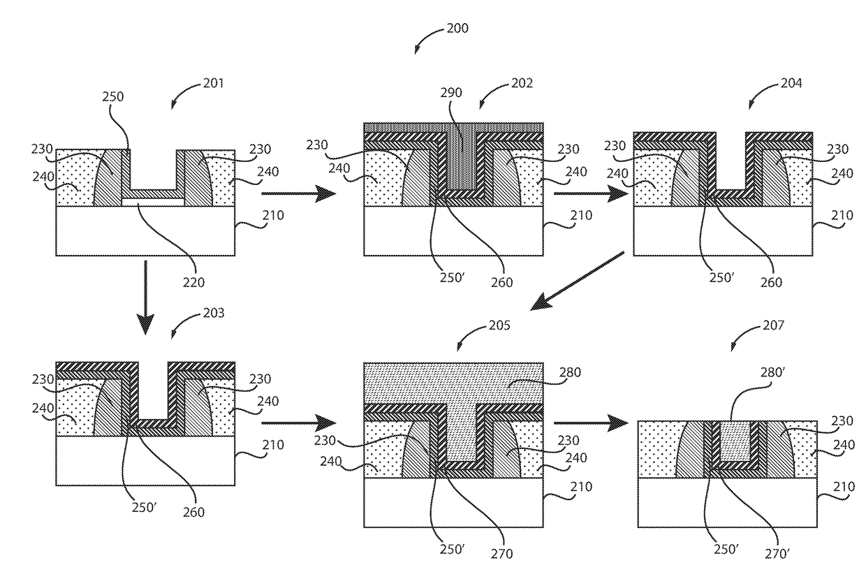
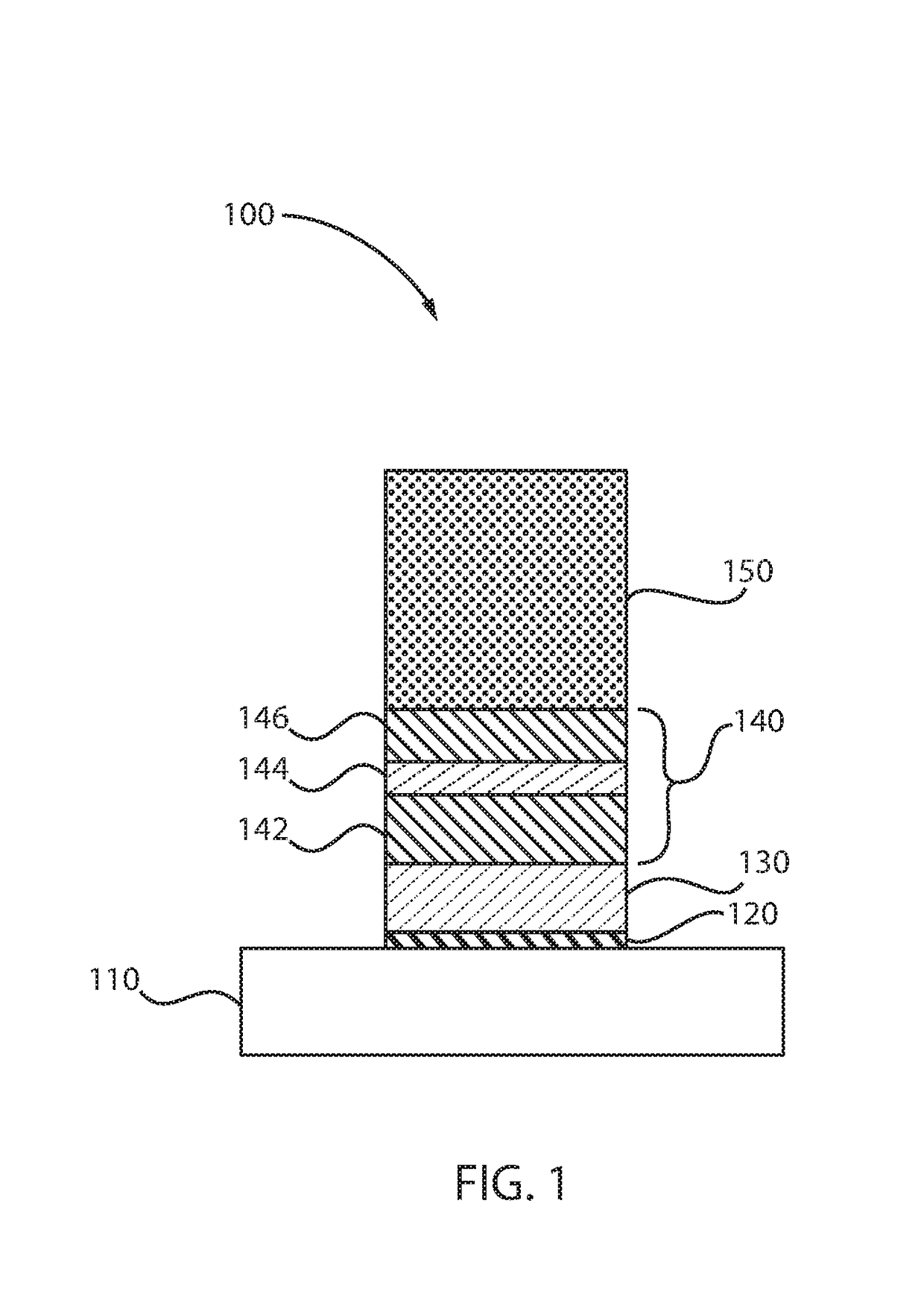
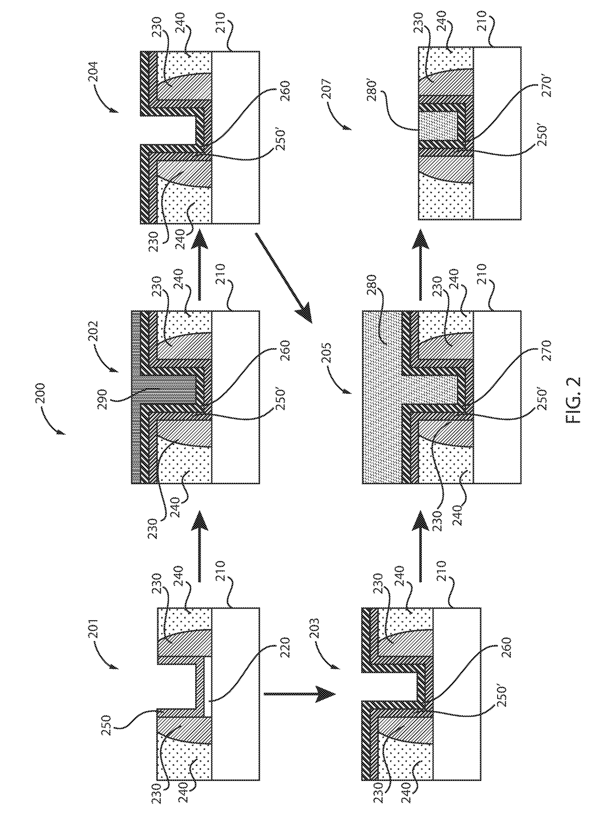
[0017]The present invention relates generally to the formation of a semiconductor device. The formation includes forming an oxygen containing interfacial layer on a semiconductor substrate, forming a hafnium oxide layer on the interfacial layer, the hafnium oxide layer crystallizing to a non-centrosymmetric phase in a final structure, forming a first electrode containing a scavenging metal, which reduces a thickness of the interfacial layer via an oxygen scavenging reaction in the final structure, on the hafnium oxide layer, and forming a second electrode on the first electrode.

[0018]The present invention relates generally to the formation of a semiconductor device. The formation includes forming an oxygen containing interfacial layer on a semiconductor substrate, forming a hafnium oxide layer on the interfacial layer, the hafnium oxide layer crystallizing to a non-centrosymmetric phase in a final structure, forming a sacrificial layer containing a scavenging metal, which reduces a ...


PUM

PropertyMeasurementUnit
dielectric constantaaaaaaaaaa
thicknessaaaaaaaaaa
thicknessaaaaaaaaaa

Abstract

A method is presented for forming a semiconductor device. The method includes forming an oxygen containing interfacial layer on a semiconductor substrate, forming a hafnium oxide layer on the interfacial layer, the hafnium oxide layer crystallizing to a non-centrosymmetric phase in a final structure, forming a first electrode containing a scavenging metal, which reduces a thickness of the interfacial layer via an oxygen scavenging reaction in the final structure, on the hafnium oxide layer, and forming a second electrode on the first electrode.

Description

BACKGROUNDTechnical Field[0001]The present invention relates generally to semiconductor devices, and more specifically, to methods and devices for reducing a thickness of an interfacial layer.Description of the Related Art[0002]In the quest for improved performance, electronic circuits are becoming denser and devices are becoming smaller. For example, the most common gate dielectric in metal-oxide semiconductor field-effect transistors (MOSFETs) has been SiO2. However, as the thickness of SiO2 approaches 15 Å, substantial issues appear, including large leakage currents through the gate dielectric, concerns about the long-term dielectric reliability, and difficulty of manufacture and thickness control. A solution to the problem is to use thick films of materials, such as hafnium oxide (HfO2) and / or zirconium oxide (ZrO2) which have a dielectric constant larger than SiO2.[0003]High-k dielectrics, such as HfO2, ZrO2, or Al2O3, have dielectric constants more than double the dielectric c...

Claims


Application Information

Patent Timeline
Patent Type & Authority Applications(United States)
IPC IPC(8): H01L29/51H01L29/49H01L29/78
CPCH01L29/516H01L29/78391H01L29/4966H01L29/513H01L29/66545H01L29/6684
Inventor ANDO, TAKASHIFRANK, MARTIN M.NARAYANAN, VIJAY
Owner INT BUSINESS MASCH CORP
Why Eureka
Try Eureka