Deposition of charge trapping layers

a charge trapping and layer technology, applied in the direction of coatings, solid-state devices, chemical vapor deposition coatings, etc., can solve the problems of pvd not being suitable for deposition in three-dimensional structures and adversely affecting its operation

Active Publication Date: 2018-05-03
ASM IP HLDG BV
View PDF5 Cites 296 Cited by
  • Summary
  • Abstract
  • Description
  • Claims
  • Application Information

AI Technical Summary

Problems solved by technology

However, the silicon nitride layer 130 displays characteristics that adversely affect its operation.
However, PVD has not shown to be suitable for deposition

Method used


Image

  • Deposition of charge trapping layers
  • Deposition of charge trapping layers
  • Deposition of charge trapping layers

Examples


Embodiment Construction

[0022]Although certain embodiments and examples are disclosed below, it will be understood by those in the art that the invention extends beyond the specifically disclosed embodiments and / or uses of the invention and obvious modifications and equivalents thereof. Thus, it is intended that the scope of the invention disclosed should not be limited by the particular disclosed embodiments described below.

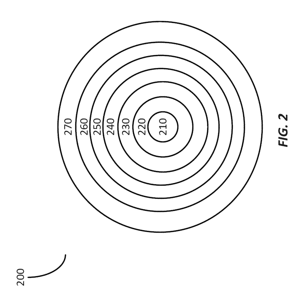
[0023]FIG. 2 illustrates a VNAND device 200 in accordance with at least one embodiment of the invention. The VNAND device 200 may comprise an oxide core or hole 210, a channel 220, a tunnel oxide layer 230, a charge trapping layer 240, a first blocking oxide 250, a second blocking oxide 260, and a control gate 270.

[0024]A status of the VNAND device may define operation of the charge trapping layer 240. When the VNAND device 200 is set to a programmed “0” status, the charge trapping layer 240 may store electrons, which may induce a shift of threshold voltage in a transistor. The charge ...


PUM

PropertyMeasurementUnit
Temperatureaaaaaaaaaa

Abstract

A semiconductor device and method for manufacturing the semiconductor device are disclosed. Specifically, the semiconductor device may include a charge trapping layer with improved retention and speed for VNAND applications. The charge trapping layer may comprise an aluminum nitride (AlN) or aluminum oxynitride (AlON) layer.

Description

CROSS REFERENCE TO RELATED APPLICATION[0001]This application claims the benefit and priority of Provisional Application No. 62 / 413,869, filed on Oct. 27, 2016, entitled “DEPOSITION OF CHARGE TRAPPING LAYERS,” the contents of which are hereby incorporated by reference to the extent the contents do not conflict with the present disclosure.FIELD OF INVENTION[0002]The present disclosure generally relates to devices and processes for manufacturing electronic devices. More particularly, the disclosure relates to charge trapping layers with improved retention and speed and the processes of forming them. Specifically, the disclosure discloses metal oxynitride films for Vertical NAND (VNAND) devices.BACKGROUND OF THE DISCLOSURE[0003]NAND devices have been in production with applications in flash memory. Specifically, NAND devices work with main stream non-volatile flash memory devices. An example of a current NAND device is a Metal-Oxide-Nitride-Oxide-Silicon (“MONOS”) cell stack. FIG. 1 ill...

Claims


Application Information

Patent Timeline
IPC IPC(8): H01L29/792H01L21/02H01L27/11524C23C16/34H01L29/66H01L27/11551
CPCH01L29/792H01L21/02227H01L27/11524H01L21/0214H01L21/02164C23C16/34H01L21/02274H01L21/0234H01L29/66833H01L27/11551C23C16/303C23C16/45529C23C16/45531H01L21/02178H01L21/0228H10B43/35H10B43/27H01L21/02172H01L21/02205H10B43/40H10B41/20H10B41/35
Inventor CALKA, PAULINEXIE, QIPIERREUX, DIETERJONGBLOED, BERT
Owner ASM IP HLDG BV
Why Eureka
Try Eureka