
Touch circuit, touch sensing device, and touch sensing method

a touch sensing device and touch circuit technology, applied in the field of display devices, can solve the problems of increasing the problem of serious problems, affecting the efficiency of charge control, and the undesirable parasitic capacitance of the touch sensing device, so as to reduce the area of the charge control circuit and improve the charge control efficiency.

Active Publication Date: 2018-06-21
LG DISPLAY CO LTD
View PDF111 Cites 10 Cited by
  • Summary
  • Abstract
  • Description
  • Claims
  • Application Information

AI Technical Summary

Benefits of technology

The present patent provides a touch circuit, sensing device, and method that can improve touch sensing performance by reducing or eliminating the influence of parasitic capacitance, which can occur inside or outside a touch screen panel. The technology can compensate for changes in charge quantity caused by parasitic capacitance and eliminate noise components from sensing data to obtain accurate touch sensing results.

Problems solved by technology

The conventional touch sensing device may generate undesirable parasitic capacitance between touch driving patterns and neighboring conductors inside or outside a touch screen panel in the process of driving and sensing the touch screen panel.
In particular, such a problem becomes more serious when a display panel has a built-in touch screen panel.

Method used


Image

  • Touch circuit, touch sensing device, and touch sensing method
  • Touch circuit, touch sensing device, and touch sensing method
  • Touch circuit, touch sensing device, and touch sensing method

Examples


Embodiment Construction

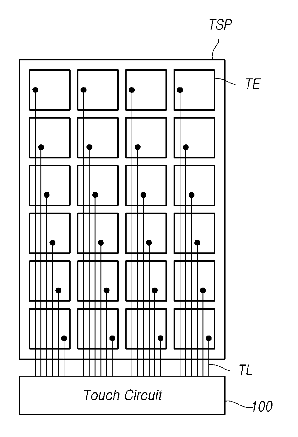
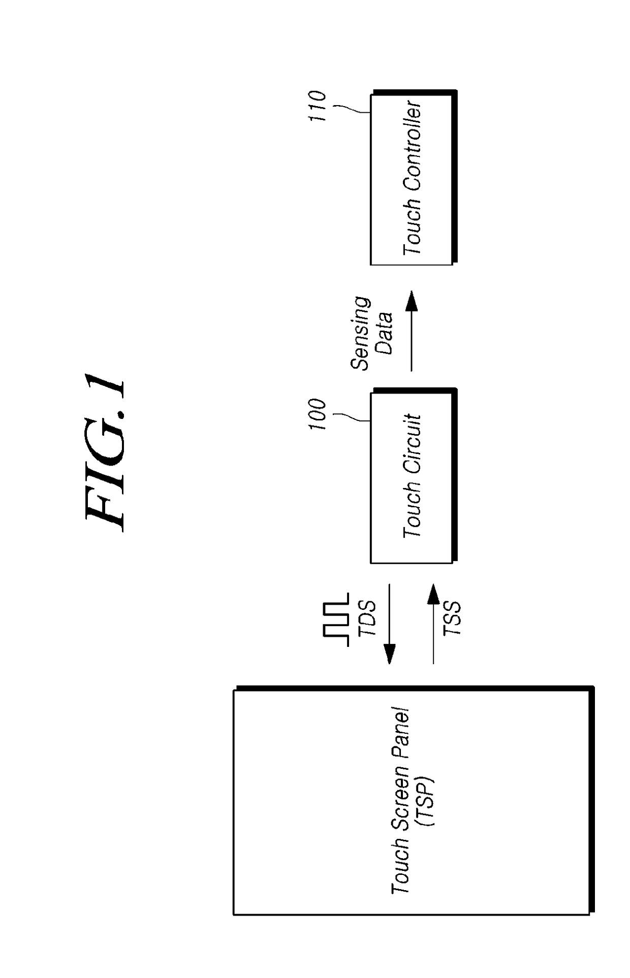
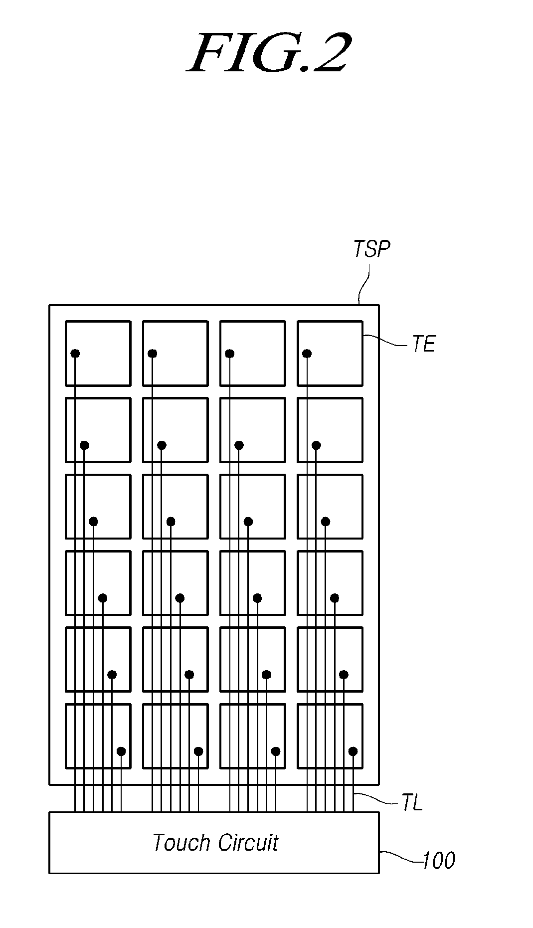
[0053]Hereinafter, embodiments of the present disclosure will be described in detail with reference to the accompanying illustrative drawings. In designating elements of the drawings by reference numerals, the same elements will be designated by the same reference numerals even when they are shown in different drawings. Further, in the following description of the present disclosure, a detailed description of known functions and configurations incorporated herein will be omitted when the same may make the subject matter of the present disclosure rather unclear.

[0054]In addition, terms, such as “first”, “second”, “A”, “B”, “(a)”, “(b)” or the like may be used herein when describing components of the present disclosure. Each of these terminologies is not used to define an essence, order or sequence of a corresponding component, but is used merely to distinguish the corresponding component from other component(s). In the case where it is described that a certain structural element “is ...


PUM


Abstract

The present disclosure relates to a touch circuit, a touch sensing device, and a touch sensing method. According to the present disclosure, it is possible to obtain an accurate touch sensing result (the presence or absence of a touch and / or a touch position) by compensating for the unintentional change in the quantity of the charge corresponding to a signal obtained by driving a touch screen panel, so as to obtain sensing data in which the influence of the parasitic capacitance generated inside or outside the touch screen panel is reduced or eliminated, thereby improving capacitance-based touch sensing performance.

Description

CROSS-REFERENCE TO RELATED APPLICATION[0001]This application claims priority from Korean Patent Application No. 10-2016-0175041, filed on Dec. 20, 2016, which is hereby incorporated by reference for all purposes as if fully set forth herein.BACKGROUNDField of the Disclosure[0002]The present disclosure relates to a display device, and more particularly, to a touch circuit, a touch sensing device, and a touch sensing method.Description of the Background[0003]With the advent of the information age, display devices for displaying an image are being increasingly required in various forms, and in recent years, various display devices, such as liquid crystal displays (LCDs), plasma display panels (PDPs), and organic light-emitting display devices (OLEDs), have come to be utilized.[0004]Among such display devices, there is a touch display device capable of providing a touch-based input method that allows a user to easily or intuitively and conveniently input information or commands, going b...

Claims


Application Information

Patent Timeline
IPC IPC(8): G06F3/044G06F3/041
CPCG06F3/044G06F3/0416G06F3/0418G06F3/0412G06F3/04182G06F2203/04111
Inventor LEE, HONGJUKANG, HYEONGWONJO, YOUNGWOO
Owner LG DISPLAY CO LTD
Learn More