Semiconductor structure and method for manufacturing semiconductor structure

a semiconductor and structure technology, applied in the direction of semiconductor/solid-state device details, semiconductor devices, radiation controlled devices, etc., can solve the problems of difficult improvement of chip package product yield, warpage of optical glass, dam elements, etc., and achieve the effect of preventing the wafer from warpag

Active Publication Date: 2018-06-21
XINTEC INC
View PDF25 Cites 2 Cited by
  • Summary
  • Abstract
  • Description
  • Claims
  • Application Information

AI Technical Summary

Benefits of technology

[0022]In the aforementioned embodiments of the present invention, since the dam element and the optical element are not disposed yet before the through hole, the trench, and the isolation layer are formed in the method for manufacturing the semiconductor structure, and the first temporary bonding layer is used to adhere the first carrier to the wafer, the first carrier can provide a sufficient supporting force to the wafer and prevents the wafer from warpage caused by a high temperature. Moreover, after the isolation layer is formed, the second temporary bonding layer may be used to adhere the second carrier to the second surface of the wafer. Through a supporting force of the second carrier to the wafer, the first carrier may be removed and the wafer is not bent to be cracked. Since there is no high temperature process after the first carrier is removed, disposing the optical element with the dam element on the first surface of the wafer does not cause warpages of the optical element, the dam element, and the wafer in a subsequent manufacturing process.

Problems solved by technology

However, since coefficient thermal expansion (CTE) of the optical glass is different from that of the dam element, warpage may occur in the optical glass, the dam element, and the wafer after a high temperature process (e.g., CVD).
Since the dam element is located outside the image sensing area, and an increase of the size of the image sensing area is referred to as a decrease of a supporting force of the dam element to the optical glass and the wafer, the warpage is prone to occur.
As a result, after chip packages are formed by dicing the stacked optical glass, dam element, and wafer, product yield of the chip packages is difficult to improve.

Method used


Image

  • Semiconductor structure and method for manufacturing semiconductor structure
  • Semiconductor structure and method for manufacturing semiconductor structure
  • Semiconductor structure and method for manufacturing semiconductor structure

Examples


Embodiment Construction

[0030]Reference will now be made in detail to the present embodiments of the invention, examples of which are illustrated in the accompanying drawings. Wherever possible, the same reference numbers are used in the drawings and the description to refer to the same or like parts.

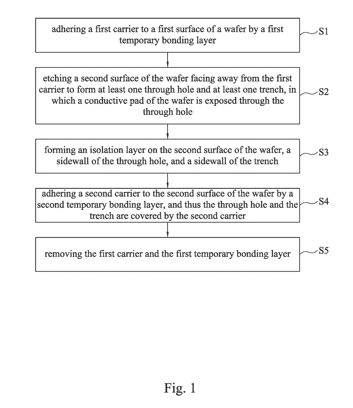
[0031]FIG. 1 is a flowchart of a method for manufacturing a semiconductor structure according to one embodiment of the present invention. The method for manufacturing the semiconductor structure includes the following steps. In step S1, a first carrier is adhered to a first surface of a wafer by a first temporary bonding layer. Thereafter, in step S2, a second surface of the wafer facing away from the first carrier is etched to form at least one through hole and at least one trench, in which a conductive pad of the wafer is exposed through the through hole. Next, in step S3, an isolation layer is formed on the second surface of the wafer, a sidewall of the through hole, and a sidewall of the trench. Afterwards...


PUM


Abstract

A method for manufacturing a semiconductor structure includes the following steps. A first carrier is adhered to a first surface of a wafer by a first temporary bonding layer. A second surface of the wafer facing away from the first carrier is etched to form at least one through hole and at least one trench, in which a conductive pad of the wafer is exposed through the through hole. An isolation layer is formed on the second surface of the wafer, a sidewall of the through hole, and a sidewall of the trench. A second carrier is adhered to the second surface of the wafer by a second temporary bonding layer, and thus the through hole and the trench are covered by the second carrier. The first carrier and the first temporary bonding layer are removed.

Description

RELATED APPLICATIONS[0001]This application claims priority to U.S. provisional Application Ser. No. 62 / 436,655, filed Dec. 20, 2016, which is herein incorporated by reference.BACKGROUNDField of Invention[0002]The present invention relates to a method for manufacturing semiconductor structure.Description of Related Art[0003]Generally, in manufacturing a semiconductor structure that has an image sensing area, an optical glass is bonded to a wafer through a dam element, and then an etching process, a chemical vapor deposition (CVD) process, a physical vapor deposition (PVD) process, an electroplating process, or a grinding process is performed to the wafer. However, since coefficient thermal expansion (CTE) of the optical glass is different from that of the dam element, warpage may occur in the optical glass, the dam element, and the wafer after a high temperature process (e.g., CVD).[0004]The aforementioned warpage is more obviously formed in a semiconductor structure that has a large...

Claims


Application Information

Patent Timeline
Patent Type & Authority Applications(United States)
IPC IPC(8): H01L27/146H01L23/00H01L21/683
CPCH01L27/14687H01L27/14685H01L27/14618H01L27/14627H01L27/1463H01L27/14632H01L27/14636H01L24/20H01L24/19H01L24/94H01L21/6835H01L2224/214H01L2924/3511H01L2221/68372H01L2221/68386H01L27/14601H01L27/14634H01L27/14683H01L27/1469H01L2221/68381H01L2924/16235H01L2224/13101H01L2224/05569H01L2224/05572H01L24/05H01L24/13H01L24/97H01L2924/00H01L2924/014H01L2924/00014
Inventor HO, YEN-SHIHLIU, TSANG-YULIN, CHIA-SHENGLAI, CHAUNG-LIN
Owner XINTEC INC
Why Eureka
Try Eureka