Driving thin-film transistor and organic light-emitting display device using the same

a thin-film transistor and display device technology, applied in the direction of transistors, static indicating devices, instruments, etc., can solve the problems of difficult to realize various and sufficient gradation, slow response speed of thin-film transistors, and difficult to achieve sufficient gradation, etc., to reduce kink effects, high resolution, and sufficient gradation

Active Publication Date: 2018-07-05
LG DISPLAY CO LTD
View PDF0 Cites 8 Cited by
  • Summary
  • Abstract
  • Description
  • Claims
  • Application Information

AI Technical Summary

Benefits of technology

[0011]A driving thin-film transistor and an organic light-emitting display device using the same according to the present invention include a stack-type active layer, thereby reducing a kink effect and enabling sufficient gradation and high resolution by increasing a channel length without increasing an area in plan.

Problems solved by technology

However, although element characteristics such as, for example, mobility of the respective thin-film transistors, are improved when the area of each sub-pixel is small, a driving thin-film transistor may undergo the saturation of current within a short time when a gate voltage is applied thereto, which makes it difficult to realize various and sufficient gradation.
In this situation, when the driving thin-film transistor has the same stack structure as the other thin-film transistors, the speed of response of the thin-film transistors is fast, but sufficient gradation is difficult because the linear section of the IDS-VG, graph is excessively short.
In addition, since a thin-film transistor having a general single gate structure exhibits a worsened kink effect, which causes increased ID, after saturation, the thin-film transistor has difficulty in securing reliability as a driving thin-film transistor that directly supplies current to an organic light-emitting diode.

Method used


Image

  • Driving thin-film transistor and organic light-emitting display device using the same
  • Driving thin-film transistor and organic light-emitting display device using the same
  • Driving thin-film transistor and organic light-emitting display device using the same

Examples


first embodiment

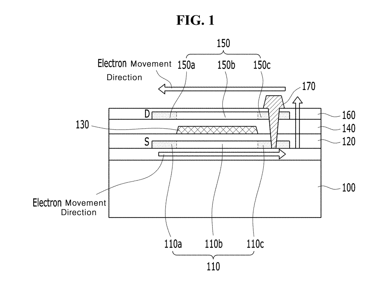
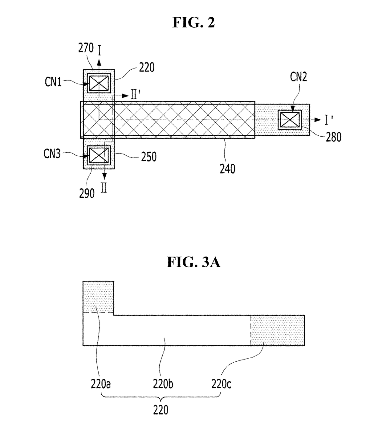
[0059]FIG. 2 is a plan view illustrating a driving thin-film transistor according to a first embodiment of the present invention, FIG. 3A is a plan view illustrating a first active layer of FIG. 2, and FIG. 3B is a plan view illustrating a second active layer of FIG. 2. In addition, FIG. 4 is a cross-sectional view taken along line I-I′ of FIG. 2 and FIG. 5 is a cross-sectional view taken along line II-II′ of FIG. 2.

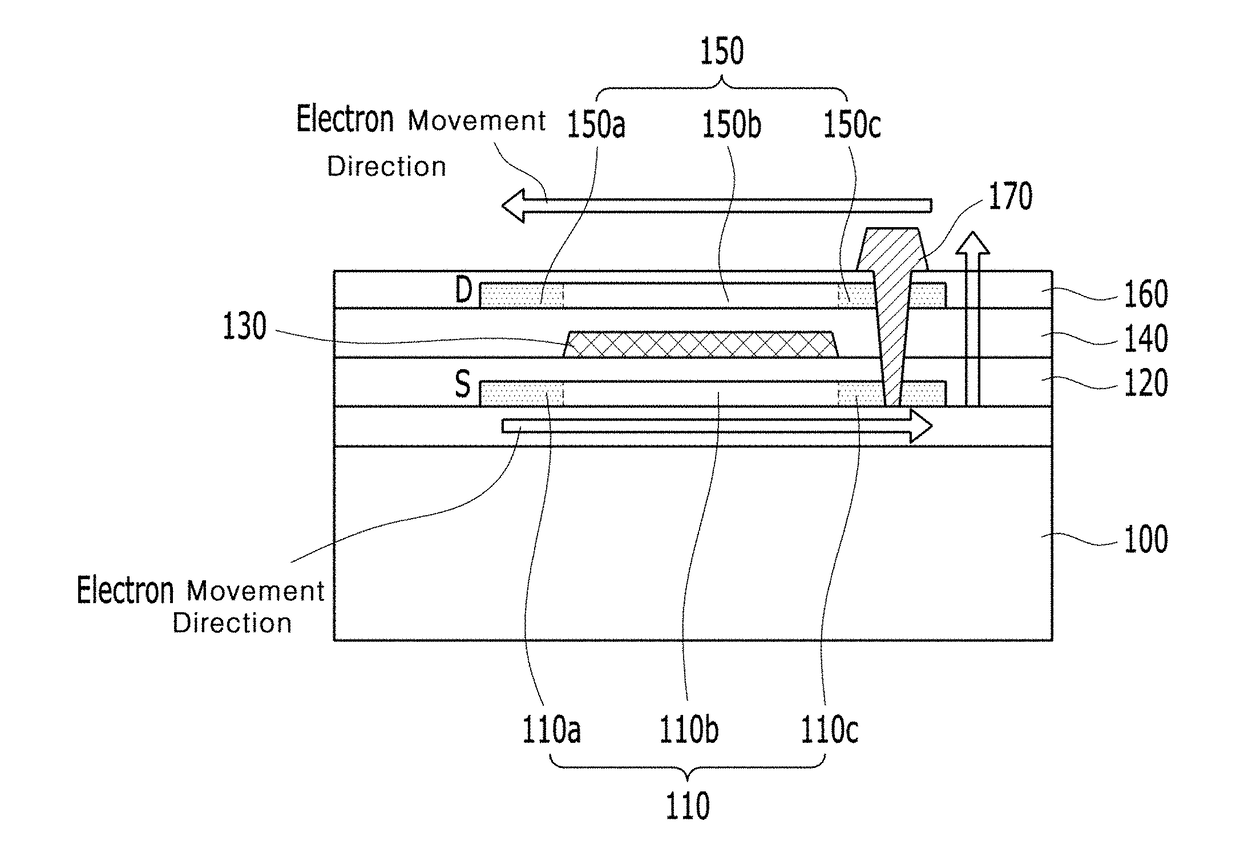
[0060]In the plan structure of the driving thin-film transistor according to the first embodiment of the present invention, as illustrated in FIGS. 2 to 5, channels 220b and 250b of first and second active layers 220 and 250 have the same area. The first and second active layers 220 and 250 have protruding portions configured to be connected to different electrodes (e.g., a source electrode 270 and a drain electrode 290), and the protruding portions are doped.

[0061]Now, the layered structure of the driving thin-film transistor will be described in sequence starting with ...

second embodiment

[0078]FIG. 6 is a plan view illustrating a driving thin-film transistor according to a second embodiment of the present invention, FIG. 7A is a plan view illustrating a first active layer of FIG. 6, and FIG. 7B is a plan view illustrating a second active layer of FIG. 6. In addition, FIG. 8 is a cross-sectional view taken along line of FIG. 6, and FIG. 9 is a cross-sectional view taken along line IV-IV′ of FIG. 6.

[0079]The driving thin-film transistor according to the second embodiment of the present invention illustrated in FIGS. 6 to 9 has the same layered structure as that of the driving thin-film transistor according to the first embodiment of the present invention described above, but differs as to the area over which a gate electrode 340 overlaps first and second active layers 320 and 350, and consequently, differs as to the length of channels provided in the first and second active layers 320 and 350.

[0080]Now, a layered structure of the driving thin-film transistor will be d...


PUM


Abstract

A driving thin-film transistor can include a substrate; a first active layer disposed on the substrate and including a first protruding portion; a second active layer overlapping with the first active layer and including a second protruding portion; a gate electrode disposed between the first active layer and the second active layer; a source electrode connected to the first protruding portion of the first active layer; and a drain electrode connected to the second protruding portion of the second active layer, in which the first protruding portion of the first active layer and the second protruding portion of the second active layer are located at different positions.

Description

[0001]This application claims the benefit of Korean Patent Application No. 10-2016-0184398, filed in the Republic of Korea on Dec. 30, 2016, which is hereby incorporated by reference as if fully set forth herein.BACKGROUND OF THE INVENTIONField of the Invention[0002]The present invention relates to a driving thin-film transistor, and more particularly, to a stack-type driving thin-film transistor, which is advantageous for super-high resolution and secures device stability, and an organic light-emitting display device using the same.Discussion of the Related Art[0003]With the development of various portable electronic apparatuses, such as mobile communication terminals and laptop computers, there is an increasing demand for flat panel display devices that may be applied thereto.[0004]As such flat panel display devices, for example, liquid crystal display devices, plasma display panel devices, field emission display devices, and organic or inorganic light-emitting display devices hav...

Claims


Application Information

Patent Timeline
Patent Type & Authority Applications(United States)
IPC IPC(8): H01L51/52H01L27/32G09G3/3225
CPCH01L51/5203H01L27/3276H01L27/3248H01L27/3209G09G3/3225G09G2310/0264H01L29/78696H10K59/1213G09G2300/0426G09G2300/0465H01L29/78612H01L29/78618H01L27/1244H01L27/1251H01L27/1222H01L29/78606H01L29/45H10K59/123H10K50/805H10K59/32H10K59/131H01L29/786
Inventor JUNG, IN-SANGOH, KUM-MIRYU, WON-SANGKO, SUN-WOOK
Owner LG DISPLAY CO LTD
Why Eureka
Try Eureka