
Configurable Computing Array Die Based on Printed Memory and Two-Sided Integration

a computing array and printed memory technology, applied in the field of integrated circuits, can solve problems such as limiting further applications of configurable gate arrays, and achieve the effect of more computing power

Inactive Publication Date: 2018-07-12
HANGZHOU HAICUN INFORMATION TECH +1
View PDF0 Cites 0 Cited by
  • Summary
  • Abstract
  • Description
  • Claims
  • Application Information

AI Technical Summary

Benefits of technology

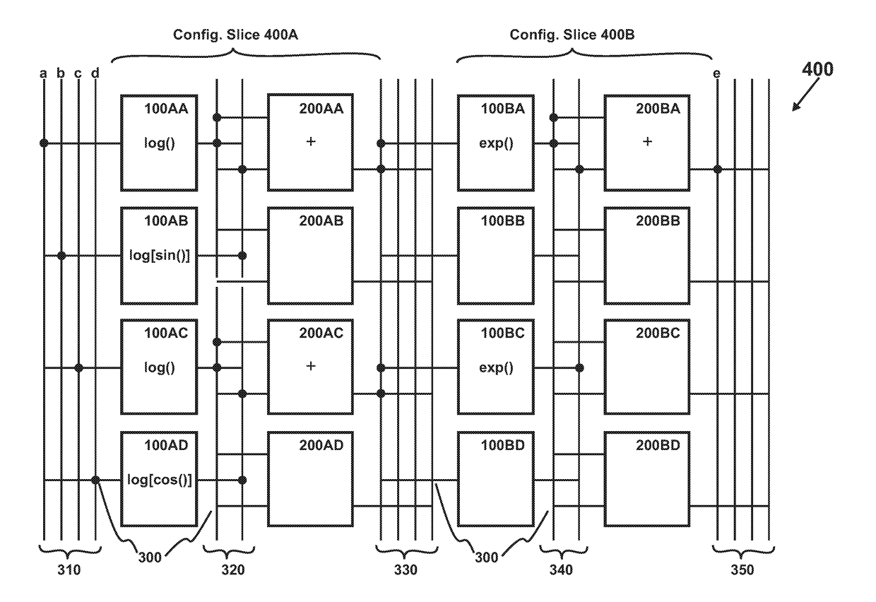
The present invention is a new type of configurable gate array that is based on two-sided integration. It is a monolithic die that includes at least an array of configurable computing elements, an array of configurable logic elements, and a plurality of configurable interconnects. Each configurable computing element can selectively realize a math function from a math library, while each configurable logic element can selectively realize a logic function from a logic library. The configurable computing elements and logic elements are formed on different sides of a semiconductor substrate and are electrically coupled through a plurality of through-silicon vias (TSV). This new configuration allows for the realization of complex math functions by selectively programming the configurable computing and logic elements.

Problems solved by technology

Apparently, fixed computing elements would limit further applications of the configurable gate array.

Method used


Image

  • Configurable Computing Array Die Based on Printed Memory and Two-Sided Integration
  • Configurable Computing Array Die Based on Printed Memory and Two-Sided Integration
  • Configurable Computing Array Die Based on Printed Memory and Two-Sided Integration

Examples


Embodiment Construction

[0023]Those of ordinary skills in the art will realize that the following description of the present invention is illustrative only and is not intended to be in any way limiting. Other embodiments of the invention will readily suggest themselves to such skilled persons from an examination of the within disclosure.

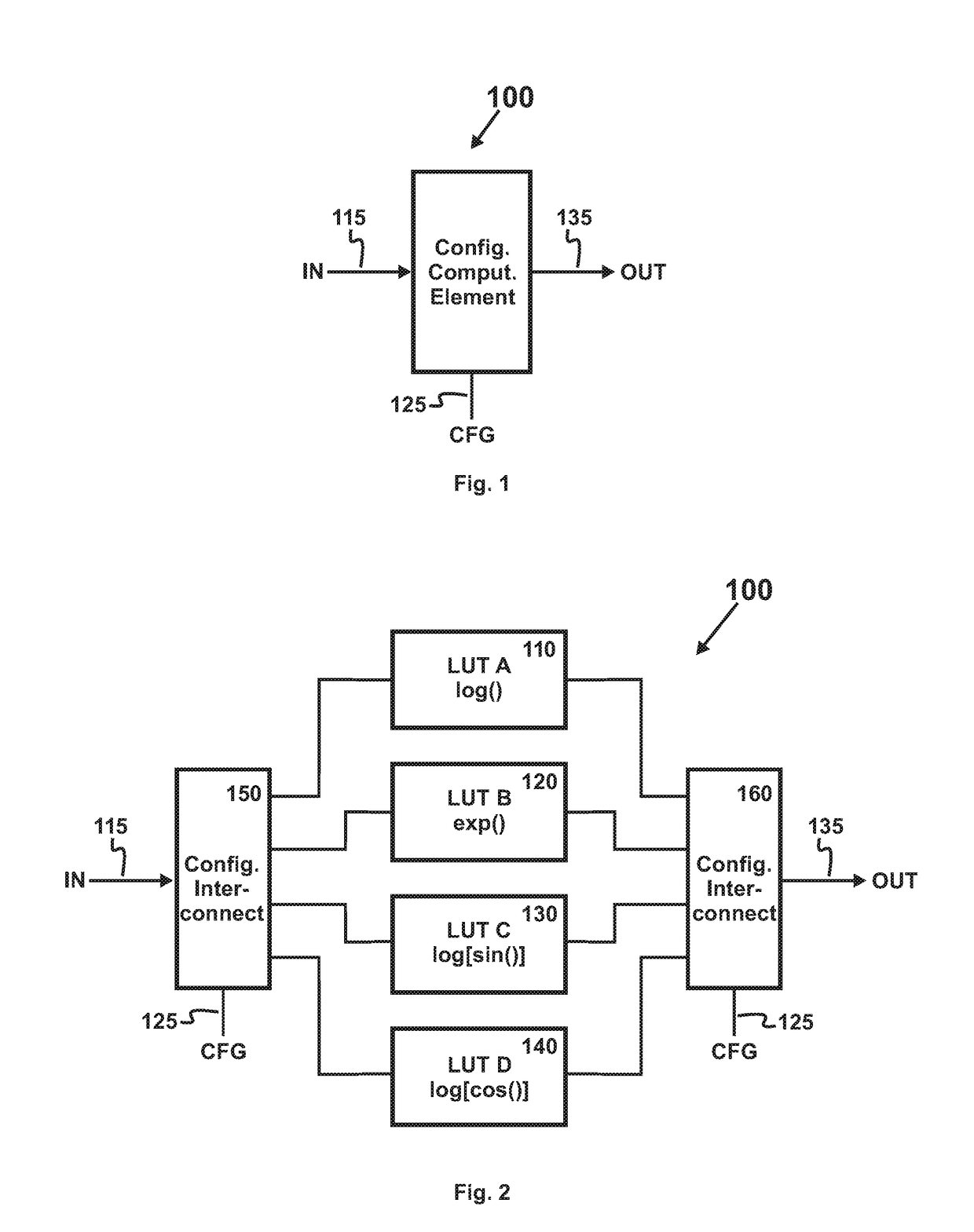
[0024]FIG. 1 discloses a symbol for a preferred configurable computing element 100. The input port IN includes input data 115, the output port OUT includes output data 135, and the configuration port CFG includes at least a configuration signal 125. The configurable computing element 100 can selectively realize a math function from a math library depending on the configuration signal 125. In the present invention, the math functions in the math library are generally referred to as basic functions and include functions such as exp, log, sin, cos, tan, a tan, sqrt, cbrt.

[0025]FIG. 2 is a circuit block diagram of a preferred configurable computing element 100. It also disclose...


PUM


Abstract

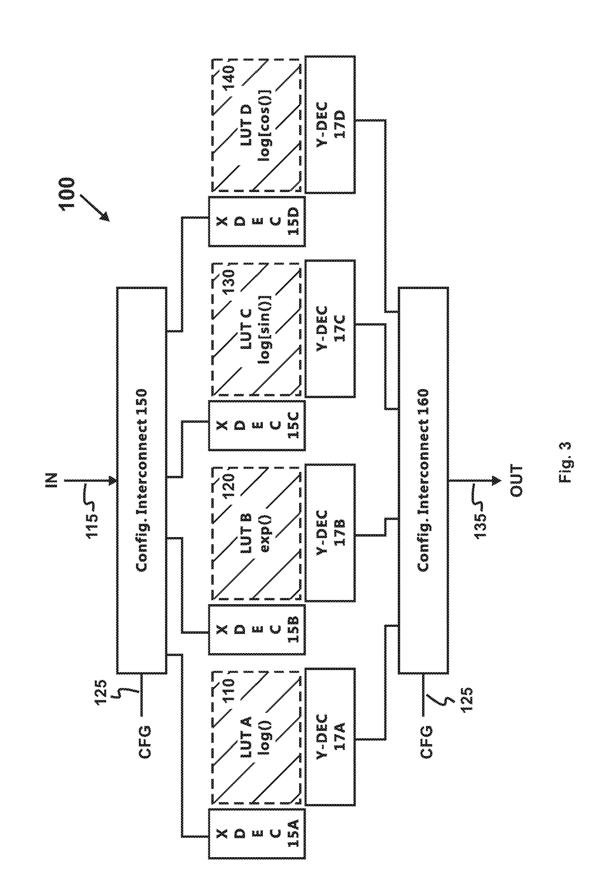
The present invention discloses a new type of configurable gate array—a configurable computing array die based on two-sided integration. It is a monolithic die and comprises at least a configurable computing element and a configurable logic element formed on different sides of a semiconductor substrate. Each configurable computing element can selectively realize a basic function from a math library. It comprises a plurality of printed arrays for storing the look-up tables (LUT) for different basic functions.

Description

CROSS-REFERENCE TO RELATED APPLICATIONS[0001]This application is a continuation-in-part of “Configurable Gate Array Based on Three-Dimensional Printed Memory”, application Ser. No. 15 / 450,017, filed Mar. 5, 2017, which claims priority from Chinese Patent Application 201610125731.8, filed on Mar. 5, 2016, in the State Intellectual Property Office of the People's Republic of China (CN), the disclosure of which is incorporated herein by reference in its entirety.[0002]This application also claims priority from Chinese Patent Application 201810187766.3, filed on Mar. 7, 2018, in the State Intellectual Property Office of the People's Republic of China (CN), the disclosure of which is incorporated herein by reference in its entirety.BACKGROUND1. Technical Field of the Invention[0003]The present invention relates to the field of integrated circuit, and more particularly to configurable gate array.2. Prior Art[0004]A configurable gate array is a semi-custom integrated circuit designed to be...

Claims


Application Information

Patent Timeline
Patent Type & Authority Applications(United States)
IPC IPC(8): H03K19/177G11C17/10G11C5/02
CPCH03K19/1776G11C17/10G11C5/02H03K19/17728
Inventor ZHANG, GUOBIAO
Owner HANGZHOU HAICUN INFORMATION TECH
Learn More