Display driver panel device and method for driving same

Active Publication Date: 2018-07-26
INTELLECT CHIP ELECTRONIC TECH CO LTD
View PDF10 Cites 1 Cited by
  • Summary
  • Abstract
  • Description
  • Claims
  • Application Information

AI Technical Summary

Benefits of technology

The present invention is a display driver panel device that allows for faster and synchronized imaging and display of an image. The device includes an image sensor array and a display driver array, each composed of a corresponding number of elements. This ensures that each pixel sensor element sends a display driver element a corresponding first display input signal. As a result, the display driver elements respond in an almost synchronized manner, effectively mitigating the slow response problem arising from row-wise scanning and input of external display driver signals to the display driver elements. Additionally, the display system incorporating the display driver panel device allows for almost synchronized array imaging and display with a significantly reduced time delay.

Problems solved by technology

However, this portable AR system is associated with some fundamental drawbacks, one of which is that there is an inevitable time delay between the real-world image 1 captured by the camera 2 and the image displayed on the HMD display screen 3, which constitute one of the causes of a viewer's vertigo.

Method used


Image

  • Display driver panel device and method for driving same
  • Display driver panel device and method for driving same
  • Display driver panel device and method for driving same

Examples


embodiment 1

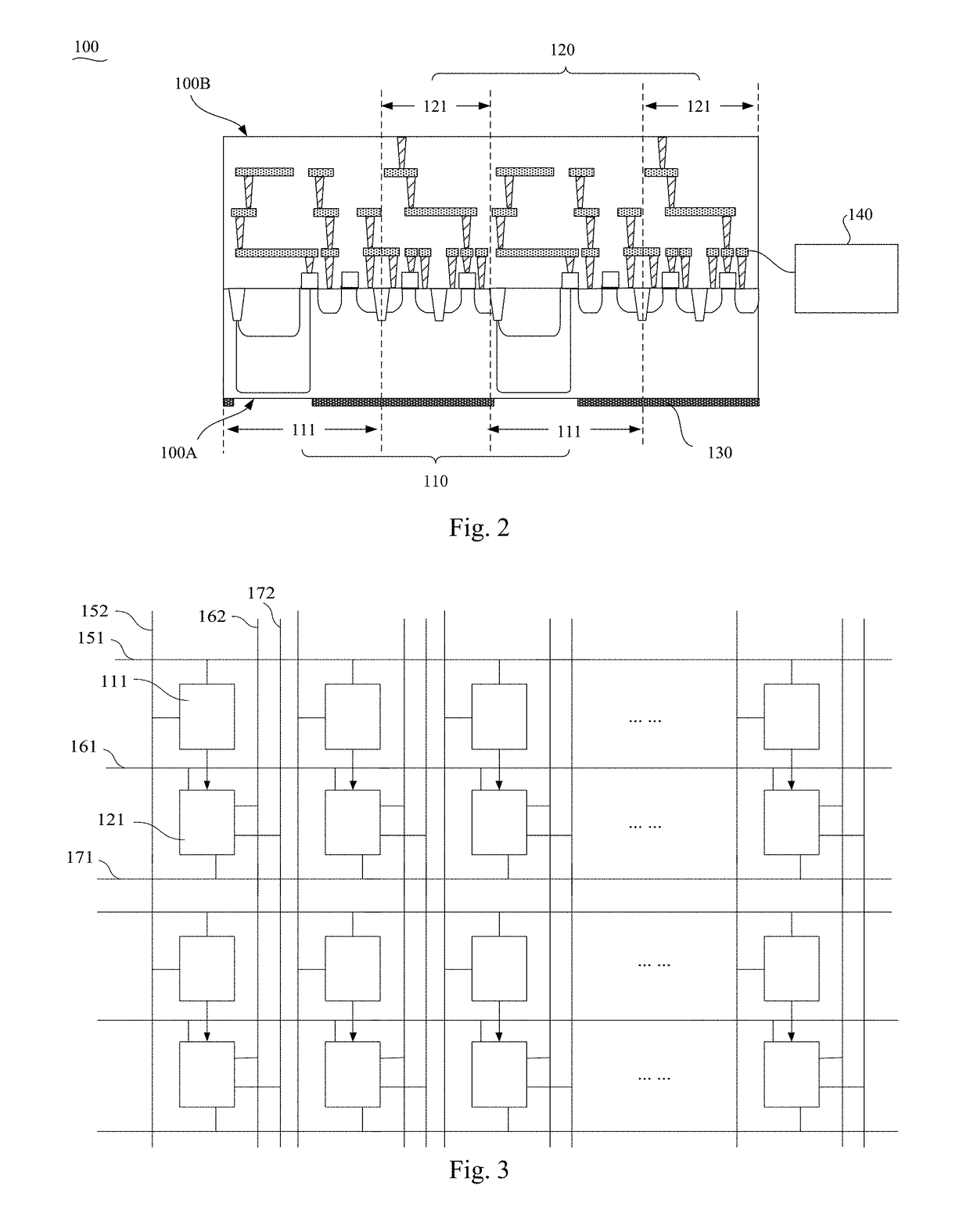
[0032]FIG. 2 is a structural schematic of a display driver panel device according to Embodiment 1 of the present invention. As shown in the figure, the display driver panel device 100 includes a substrate having a first surface 100A and a second surface 100B that is parallel to and faces away from the first surface 100A. Specifically, the display driver panel device 100 further includes:

[0033]an image sensor array 110 consisting of pixel sensor elements 111 arranged in M rows and N columns; and

[0034]a display driver array 120 consisting of display driver elements 121 arranged in M rows and N columns, wherein M is an integer, and N is an integer.

[0035]Additionally, the image sensor array 110 and the display driver array 120 are both disposed in the substrate, and the display driver elements 121 are electrically connected to the respective corresponding pixel sensor elements 111.

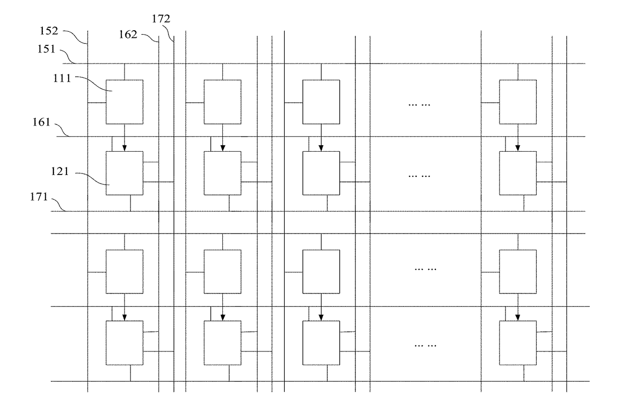
[0036]FIG. 3 shows a circuit schematic of the display driver panel device according to Embodiment 1 of the ...

embodiment 2

[0054]This embodiment differs from Embodiment 1 in that the image sensor array is arranged in parallel to the display driver array so that the pixel sensor elements and the display driver elements are arranged in two parallel planes and interconnected in a one-to-one manner.

[0055]FIG. 4 is a structural schematic of a display driver panel device according to Embodiment 2 of the present invention. As shown in FIG. 4, the display driver panel device 100′ includes:

[0056]an image sensor array 110′ consisting of pixel sensor elements 111′ arranged in M rows and N columns, wherein the image sensor array 110′ is disposed in a substrate in a parallel manner and is proximal to a first surface 100A′ of the substrate; and

[0057]a display driver array 120′ consisting of display driver elements 121′ arranged in M rows and N columns, wherein the display driver array 120′ is disposed in the substrate in a parallel manner and is proximal to a second surface 100B′ of the substrate.

[0058]Similarly to E...

embodiment 3

[0062]The display driver panel devices according to the present invention can each be incorporated in a display apparatus. This embodiment is described in detail in context of the display driver panel device 100 according to Embodiment 1 as an example.

[0063]FIG. 5 is a structural schematic of a display apparatus according to Embodiment 3 of the present invention, and FIG. 6 schematically shows how the display apparatus according to Embodiment 3 of the present invention works. With combined reference to FIGS. 5 and 6, the display apparatus 20 includes the above-described display driver panel device 100 and an array display 200. The display driver panel device 100 includes a substrate having a first surface 100A and a second surface 100B. Reference can be made to the description of Embodiment 1 for structural details of the display driver panel device 100, and further description in this regard is not necessary. The array display 200 is disposed on the second surface 100B of the subst...


PUM


Abstract

A display driver panel device and a method therefor are disclosed. The device includes: an image sensor array consisting of pixel sensor elements arranged in M rows and N columns; and a display driver array consisting of display driver elements arranged in M rows and N columns. Each of the display driver elements corresponds to a respective one of the pixel sensor elements. As such, first display input signals generated by the pixel sensor elements from a received external imaging radiation can be sent to the respective corresponding display driver elements. As a result, the display driver elements respond at the same time, resulting in an increased response speed of the display driver panel device.

Description

CROSS-REFERENCES TO RELATED APPLICATIONS[0001]This application claims the priority of Chinese patent application number 2017100600964, filed on Jan. 24, 2017, the entire contents of which are incorporated herein by reference.TECHNICAL FIELD[0002]The present invention relates to the field of image sensors and, in particular, to a display driver panel device and a method for driving the device.BACKGROUND[0003]Augmented reality (AR) is a novel technique that seamlessly combines real-world information with virtual-world information. With AR, virtual simulations of tangible information (visual information, sounds, tastes, tactile feelings, etc.) that would be rarely experienced in a certain spatial or temporal range in the real world generated by digital signal processing, computer and other techniques are overlaid on real world and perceived by human senses so as to provide a sensory experience of augmented reality. The virtual objects are overlaid in real time on the same scene or spac...

Claims


Application Information

Patent Timeline
IPC IPC(8): G09G3/36G06T11/60
CPCG09G3/3648G06T11/60G09G3/3208G09G3/3611G09G2320/0261G09G2360/14
Inventor WANG, XIAOCHUAN
Owner INTELLECT CHIP ELECTRONIC TECH CO LTD
Why Eureka
Try Eureka