Unlock instant, AI-driven research and patent intelligence for your innovation.

Pixel structure and manufacturing method thereof

a pixel structure and manufacturing method technology, applied in static indicating devices, non-linear optics, instruments, etc., can solve the problems of poor view angle characteristic of liquid crystal display using pixel structure, significant application limitation, and poor view angle characteristic of pixel structure, so as to improve the view angle and color shift of vertical alignment.

Active Publication Date: 2018-08-02
SHENZHEN CHINA STAR OPTOELECTRONICS TECH CO LTD
View PDF1 Cites 3 Cited by
  • Summary
  • Abstract
  • Description
  • Claims
  • Application Information

AI Technical Summary

Benefits of technology

The present invention provides a pixel structure and a manufacturing method for a vertical alignment liquid crystal display that improves view angle and color shift. The pixel structure includes two pixel electrodes that are not connected to each other, which are separately connected to data lines through thin-film transistors. In normal display, the two data lines are respectively applied with different voltages to set the two pixel electrodes at different potentials. This results in multiple polar angles in the liquid crystal, reducing the amount of phase difference and improving the view angle and color shift of the display. The manufacturing method is easy to conduct, and the pixel structure allows for the desired improvement in view angle and color shift.

Problems solved by technology

However, compared to cathode ray tube displays, the thin-film transistor liquid crystal display (TFT-LCD) has a relatively narrow view angle and this imposes significant limitation to the application thereof in the field of high-end displays, where the requirement for view angle is more severe, such as the fields of aviation and aeronautics and medicine.
Specifically speaking, the greater the view angle of observation is, the lower the screen brightness will be, so that the view angle characteristic of a liquid crystal display that uses the pixel structure is poor.

Method used


Image

  • Pixel structure and manufacturing method thereof
  • Pixel structure and manufacturing method thereof
  • Pixel structure and manufacturing method thereof

Examples


Embodiment Construction

[0065]To further expound the technical solution adopted in the present invention and the advantages thereof, a detailed description will be given with reference to the preferred embodiments of the present invention and the drawings thereof.

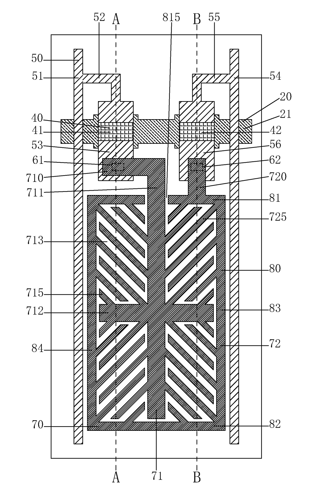
[0066]Referring to FIGS. 2-10, the present invention provides a pixel structure, which comprises a backing plate 10, a first metal layer 20 arranged on the backing plate 10, a first insulation layer 30 arranged on the first metal layer 20 and the backing plate 10, a semiconductor layer 40 arranged on the first insulation layer 30, a second metal layer 50 arranged on the semiconductor layer 40 and the first insulation layer 30, a second insulation layer 60 arranged on the second metal layer 50, the semiconductor layer 40, and the first insulation layer 30, and a transparent conductive layer 70 arranged on the second insulation layer 60.

[0067]As shown in FIG. 5, the first metal layer 20 comprises a scan line 21.

[0068]As shown in FIG. 7, the semicond...


PUM


Abstract

The present invention provides a pixel structure and a manufacturing method thereof. The pixel structure according to the present invention is such that two pixel electrodes that are not connected to each other are arranged in a single pixel structure and the two pixel electrodes are respectively connected to two data lines through respective thin-film transistors. In normal displaying, the two data lines are respectively applied with different voltages so that the two pixel electrodes are respectively set at different potentials. The different potentials of the two pixel electrodes cause liquid crystal molecules that are close to different ones of the pixel electrodes to show different polar angles so as to achieve distribution and existence of multiple polar angles in the liquid crystal, reducing the amount of phase difference of liquid crystal in different directions and thus improving the view angle and color shift of a vertical alignment liquid crystal display. The manufacturing method of the pixel structure according to the present invention is such that a manufacturing operation can be conducted easily and a pixel structure so manufactured allows for, in normal displaying, achievement of distribution and existence of multiple polar angles in liquid crystal, reducing the amount of phase difference of liquid crystal in different directions and thus improving the view angle and color shift of a vertical alignment liquid crystal display.

Description

BACKGROUND OF THE INVENTION1. Field of the Invention[0001]The present invention relates to the field of display technology, and more particular to a pixel structure and a manufacturing method thereof.2. The Related Arts[0002]With the development of the display technology, flat panel display devices, such as liquid crystal display (LCD), due to various advantages, such as high image quality, low power consumption thin device body, and wide applications, have been widely used in various consumer electronic devices, such as mobile phones, televisions, personal digital assistants, digital cameras, notebook computers, and desktop computers, or screens, and becomes a mainstream of display devices.[0003]Most of the liquid crystal display devices that are currently available in the market are backlighting liquid crystal displays, which comprise a liquid crystal display panel and a backlight module. The working principle of the liquid crystal display panel is that with liquid crystal molecul...

Claims


Application Information

Patent Timeline
IPC IPC(8): G02F1/1343G02F1/1362G02F1/1333
CPCG02F1/1343G02F1/136286G02F1/133345G09G2300/0439G02F1/134309G02F1/133707G02F1/134363G02F2201/123G02F1/134345
Inventor HAO, SIKUN
Owner SHENZHEN CHINA STAR OPTOELECTRONICS TECH CO LTD