Handling thin wafer during chip manufacture

a technology of electronic chips and wafers, applied in semiconductor devices, semiconductor/solid-state device details, electrical devices, etc., can solve the problems of becoming more and more difficult to handle thinner and thinner wafers and electronic chips, and achieve the effect of small thickness

Inactive Publication Date: 2018-08-16
INFINEON TECH AG
View PDF12 Cites 4 Cited by
  • Summary
  • Abstract
  • Description
  • Claims
  • Application Information

AI Technical Summary

Benefits of technology

[0013]According to an exemplary embodiment of the invention, a method of manufacturing semiconductor devices is provided in which a wafer is first recessed from a front side and is then thinned from a back side after having connected the wafer to a first temporary holding body. After this thinning, which may also accomplish singularization of the electronic chips of the wafer, a second temporary holding body may be attached to the back side (at which thinning has occurred), and the first temporary holding body may then be removed. Alternatively, singularization may also be achieved by front side cutting after back side thinning. By such an architecture, it can be accomplished that the sensitive thinned electronic chips and / or wafer remain(s) always attached to at least one temporary holding body, which significantly simplifies handling and protects the thin electronic chips or the thin wafer from damage. Thus, the described architecture allows to manufacture (in particular non-encapsulated or naked) semiconductor devices with significantly thinner thicknesses as can be achieved conventionally. Therefore, the manufacturing architecture promotes miniaturization of electronic chips without increasing the risk of damage of the sensitive thin electronic chips.DESCRIPTION OF FURTHER EXEMPLARY EMBODIMENTS
[0039]In an embodiment, the electrically conductive interconnect structures are embedded at least partially in the temporary holding body. They may be embedded sufficiently loose so that the electrically conductive interconnect structures remain attached on the electronic chips upon detaching the temporary holding body from the electronic chips. By the embedding of the protruding electrically conductive interconnect structures (which may involve a deformation of a foil-type first temporary holding body), the contact between the first temporary holding body and the constituents on the front side of the wafer with redistribution layer and electrically conductive interconnect structures thereon may be rendered reliable. The solder balls protruding beyond the rest of the surface of the electronic chips may therefore be temporarily placed in an interior of the first temporary holding body. This can for instance be accomplished by a sufficiently soft and / or deformable first temporary holding body or by a temporary holding body having permanent recesses at the positions of the electrically conductive interconnect structures. By both methods it can be ensured that a planar structure is obtained by the wafer with electrically conductive interconnect structures and first temporary holding body attached thereto, which simplifies grinding.

Problems solved by technology

Moreover, it becomes more and more challenging to handle thinner and thinner wafers and electronic chips.

Method used


Image

  • Handling thin wafer during chip manufacture
  • Handling thin wafer during chip manufacture
  • Handling thin wafer during chip manufacture

Examples


Embodiment Construction

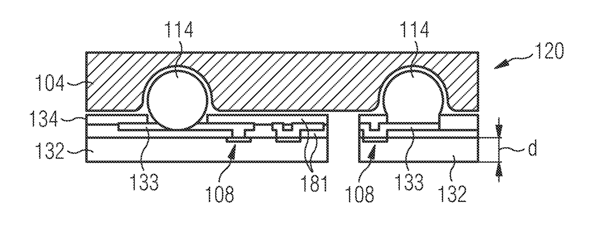
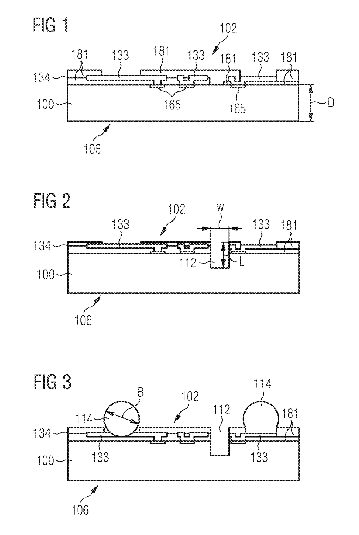
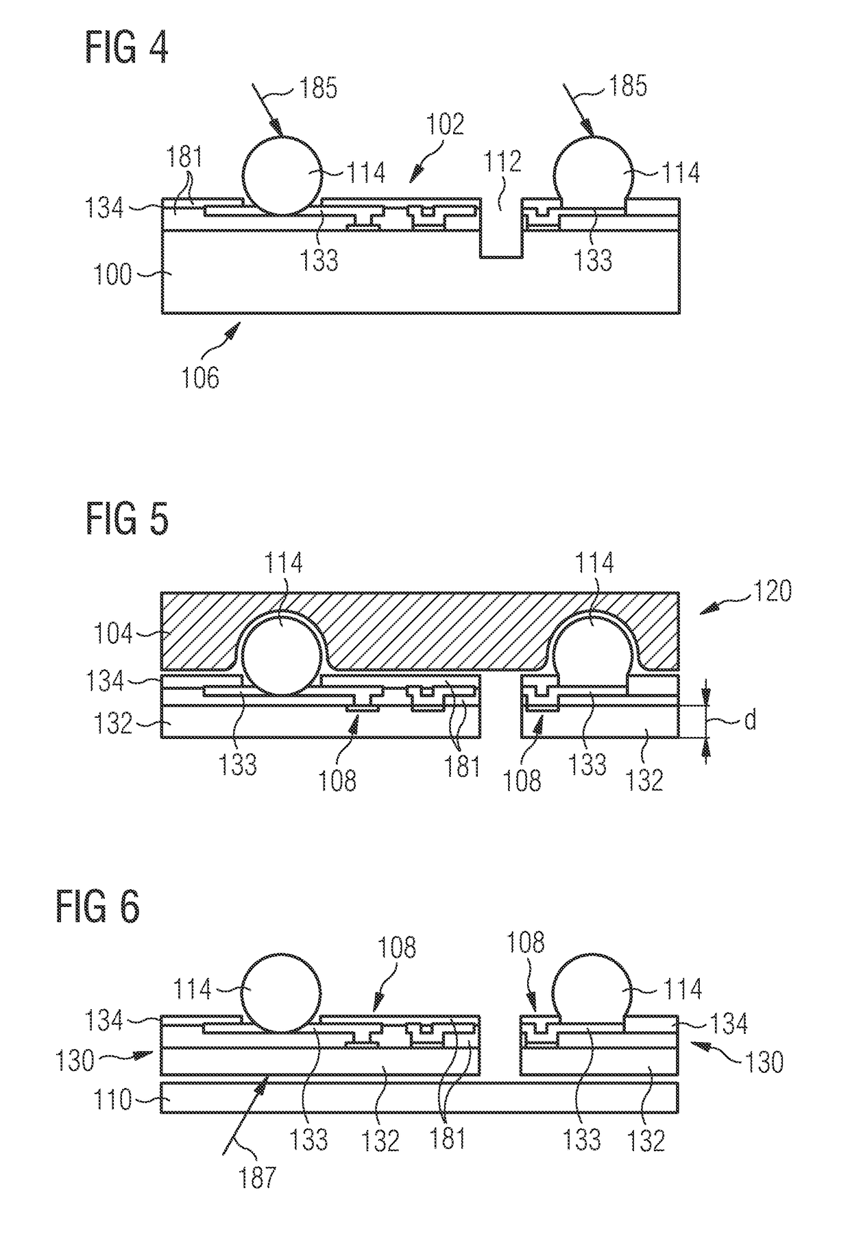
[0014]In the context of the present application, the term “temporary holding body” may particularly denote a body (such as a flexible foil) which temporarily holds a wafer and / or individual electronic chips during manufacturing semiconductor devices, but does not form part of the readily manufactured semiconductor devices. Thus, the one or more temporary holding bodies (which may also denoted as temporary carrier in certain embodiments) may be removed from the wafer or the electronic chips after temporary adhesion thereon. The temporary holding body / bodies may hold or support wafer or chips and may therefore simplify their handling, especially when wafer or chips are already very thin. A deformable temporary carrier may also cover a surface of wafer or chips and may therefore protect the latter from chemical or mechanical impact during processing, for instance during grinding.

[0015]In the context of the present application, the term “non-encapsulated semiconductor device” may partic...


PUM


Abstract

A manufacturing method is provided which comprises forming recesses in a front side of a wafer, connecting a first temporary holding body to the front side of the recessed wafer, thereafter thinning the wafer from a back side, connecting a second temporary holding body to the back side, and thereafter removing the first temporary holding body.

Description

CROSS-REFERENCE TO RELATED APPLICATION[0001]This Utility Patent Application claims priority to German Patent Application No. 10 2017 103 095.6, filed Feb. 15, 2017, which is incorporated herein by reference.BACKGROUND OF THE INVENTIONField of the Invention[0002]The present invention relates to manufacturing methods, an intermediate product, a semiconductor device, and an electronic device.Description of the Related Art[0003]Conventional packages, such as mold structures, for electronic chips have evolved to a level where the package no longer significantly impedes the performance of the electronic chips. Moreover, processing electronic chips on wafer level is a known procedure for efficiently producing them. Etching electronic chips is a conventional technique for removing material therefrom. Encapsulating electronic chips during package manufacture may protect them against the environment.[0004]In another technology, non-encapsulated semiconductor devices are used in which a redist...

Claims


Application Information

Patent Timeline
Patent Type & Authority Applications(United States)
IPC IPC(8): H01L23/00H01L21/3065H01L21/683H01L21/78H01L23/544
CPCH01L24/11H01L24/94H01L24/14H01L21/3065H01L21/6836H01L21/78H01L23/544H01L2224/023H01L21/6835H01L21/76895H01L23/5386H01L2221/68368H01L24/05H01L24/13H01L2221/68327H01L2221/6834H01L2221/68381H01L2224/0239H01L2224/024H01L2224/0401H01L2224/05099H01L2224/05548H01L2224/11334H01L2224/13007H01L2224/13021H01L2224/13024H01L2224/131H01L2224/16221H01L2224/16238H01L2224/81097H01L2224/94H01L2924/1304H01L2224/11H01L2924/00014H01L2924/014
Inventor KILLER, THOMASBRUNNBAUER, MARKUSJANKER, MARINAKOLLER, ADOLFMAIER, GABRIELMUELLER-HIPPER, ANDREASSTUECKJUERGEN, ANDREASTHOMS, CHRISTINE
Owner INFINEON TECH AG
Why Eureka
Try Eureka