Optical device

a technology of optical devices and polarizing plates, applied in static indicating devices, non-linear optics, instruments, etc., can solve the problems of low light utilization efficiency and more than half of the light used for display, and achieve the effect of reducing the proportion of regions

Active Publication Date: 2018-08-23
SHARP KK
View PDF0 Cites 7 Cited by
  • Summary
  • Abstract
  • Description
  • Claims
  • Application Information

AI Technical Summary

Benefits of technology

[0049]According to an embodiment of the present invention, in an optical device including an optical layer containing shape-anisotropic particles, it is possible to reduce the proportion of regions in which no shape-anisotropic particles are present within pixels.

Problems solved by technology

However, as the majority of liquid crystal panels are of a type that utilizes a polarizing plate, more than half of the light used for the display is absorbed by the polarizing plate.
As a result, the light utilization efficiency is low.

Method used


Image

  • Optical device
  • Optical device
  • Optical device

Examples


first embodiment

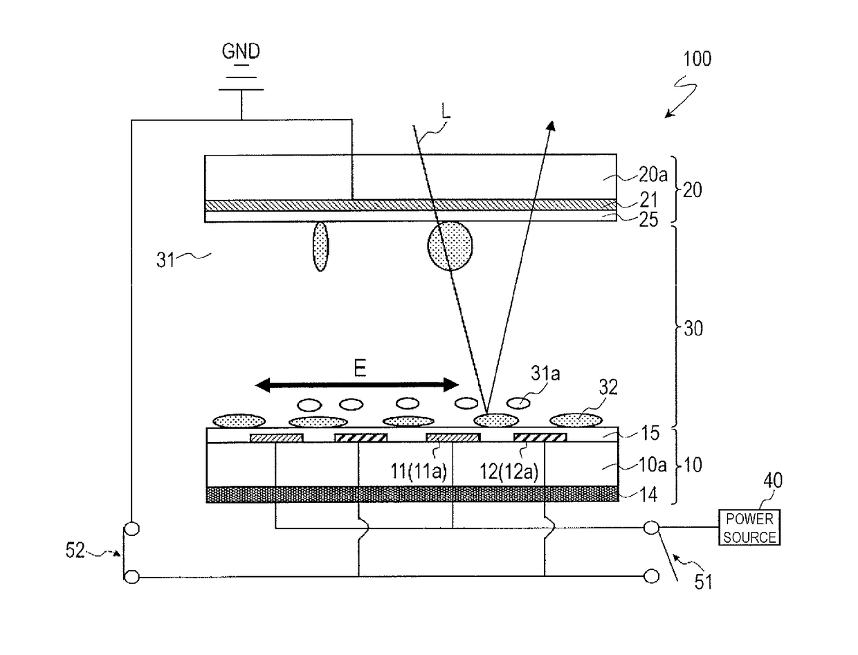
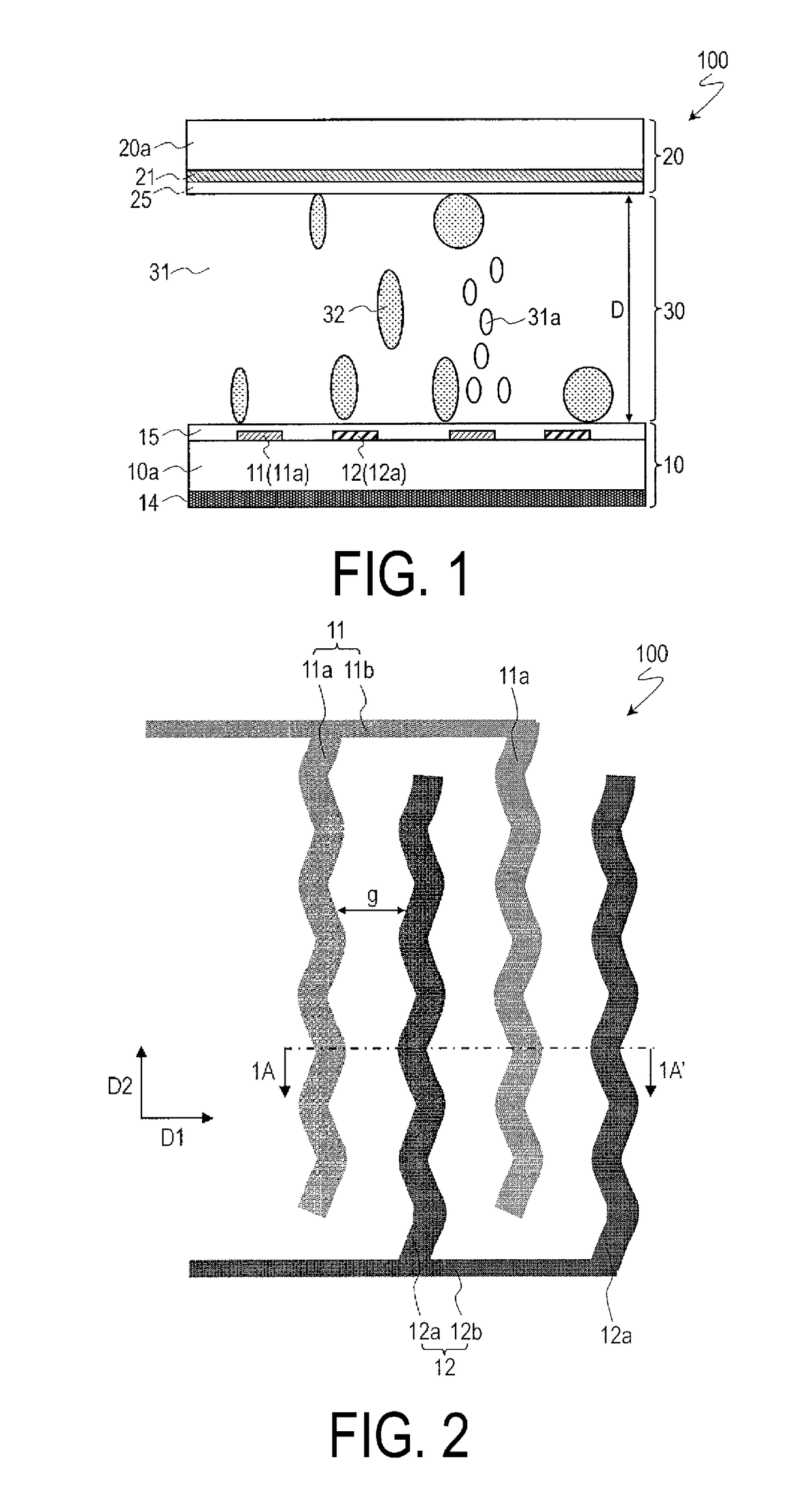
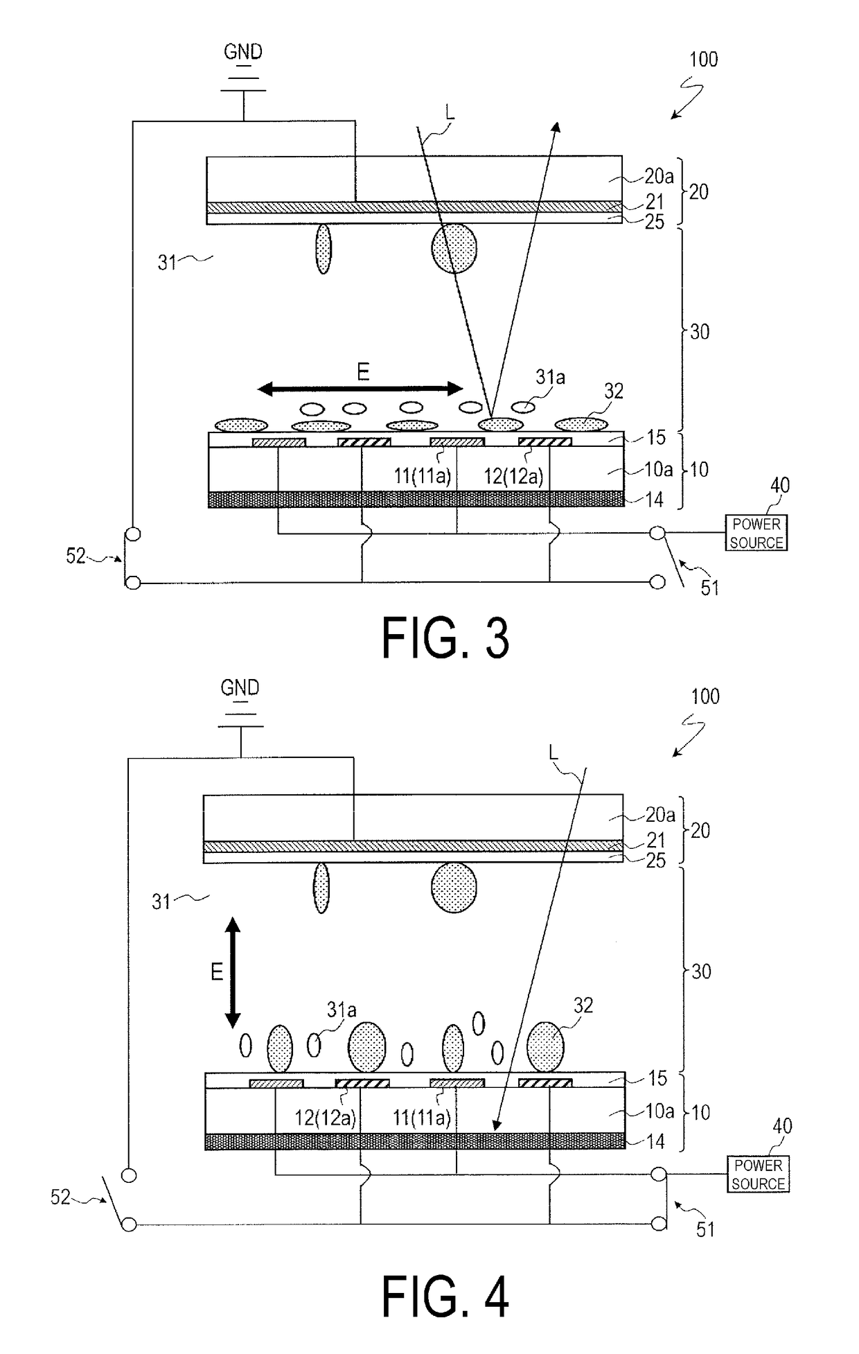
[0110]FIG. 1 and FIG. 2 illustrate a display device (optical device) 100 according to the present embodiment. FIG. 1 and FIG. 2 are a cross-sectional view and a plan view schematically illustrating the display device 100, respectively. FIG. 1 is a cross-sectional view taken along the line 1A-1A′ in FIG. 2.

[0111]The display device 100 is a reflective display device capable of performing display in a reflection mode using externally incident light (ambient light). The display device 100 includes a plurality of pixels arranged in a matrix.

[0112]As illustrated in FIG. 1, the display device 100 may include a first substrate 10 and a second substrate 20 provided opposite to each other, and an optical layer (display medium layer) 30 provided between the first substrate 10 and the second substrate 20. Hereinafter, the first substrate 10 relatively located on the rear side of the first substrate 10 and the second substrate 20 may be referred to as a “rear side substrate”, and the second subs...

second embodiment

[0173]FIG. 18 and FIG. 19 illustrate a display device (optical device) 200 of the present embodiment. FIG. 18 and FIG. 19 are a cross-sectional view and a plan view schematically illustrating the display device 200, respectively. Hereinafter, the description will be focused on the differences between the display device 200 according to the present embodiment and the display device 100 of the first embodiment.

[0174]The display device 200 according to the present embodiment differs from the display device 100 of Example 1 in that the first substrate 10 further includes a third electrode 13 provided below the first electrode 11 and the second electrode 12 with an insulating layer 16 interposed therebetween.

[0175]The third electrode 13 may be what is referred to as a solid electrode in which no slit or cutout portion is formed. The third electrode 13 may be formed of a transparent conductive material such as ITO or IZO. The thickness of the third electrode 13 may, for example, be 100 nm...

third embodiment

[0213]FIG. 30 and FIG. 31 illustrate a display device (optical device) 300 according to the present embodiment. FIG. 30 and FIG. 31 are a cross-sectional view and a plan view schematically illustrating the display device 300, respectively. Hereinafter, the description will be focused on the differences between the display device 300 according to the present embodiment and the display device 100 of the first embodiment.

[0214]In the display device 300 of the present embodiment, each of the plurality of comb teeth portions 11a of the first electrode 11 is linear, and each of the plurality of comb teeth portions 12a of the second electrode 12 is also linear. Also in the display device 300 of the present embodiment, the first substrate 10 may include a plurality of dielectric layers 17 provided so as to overlap with the outer edge of each comb tooth portion of the first electrode 11 and the outer edge of each comb tooth portion 12a of the second electrode 12. As the material for the plur...


PUM

PropertyMeasurementUnit
thicknessesaaaaaaaaaa
dielectric constantaaaaaaaaaa
diameteraaaaaaaaaa

Abstract

The optical device (100) includes a first substrate (10), a second substrate (20), and an optical layer (30). The first substrate includes a first electrode (11) and a second electrode (12) configured to be provided with mutually different electrical potentials within a pixel. The optical layer may include a medium (31) and a plurality of shape-anisotropic particles (32) dispersed in the medium. At least one of the first electrode and the second electrode may include a plurality of comb teeth portions (11a, 12a) arranged at predetermined intervals along the first direction (D1). When an electric potential difference is applied between the first electrode and the second electrode, the pixel may be configured to have an electrical field distribution in which a strong electric field region having a stronger field intensity than another region is periodically formed parallel to the surface of the optical layer along a second direction (D2) orthogonal to the first direction.

Description

TECHNICAL FIELD[0001]The present invention relates to an optical device, and more particularly relates to an optical device having an optical layer including shape anisotropic particles.BACKGROUND ART[0002]There is demand for high contrast ratios and high light utilization efficiencies in optical devices that control transmittance (or reflectivity) of incident light.[0003]Liquid crystal panels are well known as optical devices that control light transmittance by applying voltage. Liquid crystal panels generally include a pair of substrates and a liquid crystal layer provided between the substrates. In liquid crystal panels, the alignment of the liquid crystal molecules varies according to the magnitude of the voltage applied to the liquid crystal layer, such that the transmittance of light incident on the liquid crystal panel changes. As liquid crystal panels can achieve substantially high contrast ratios, they are widely used as display devices.[0004]However, as the majority of liq...

Claims


Application Information

Patent Timeline
Patent Type & Authority Applications(United States)
IPC IPC(8): G02F1/167G02F1/17G02F1/16756G02F1/166
CPCG02F1/17G02F1/167G02F1/134363G02F1/172G02F1/16756G02F1/166G02F1/1336G02F2201/124G09G3/344G09G3/3446
Inventor TERANISHI, TOMOKOMORIWAKI, HIROYUKISATOH, EIJIOHTAKE, TADASHIYOSHIDA, HIDEFUMIMATSUMURA, SATOSHI
Owner SHARP KK
Why Eureka
Try Eureka