Method of Manufacturing a Semiconductor Device

a manufacturing method and technology of semiconductor devices, applied in the direction of semiconductor devices, basic electric elements, electrical appliances, etc., can solve the problems of poor film quality and difficulty in multi-level cell operation, and achieve the effect of increasing the grain size of polycrystalline thin films, reducing interfacial state effectively, and enhancing device reliability

Active Publication Date: 2018-08-23
INST OF MICROELECTRONICS CHINESE ACAD OF SCI
View PDF0 Cites 8 Cited by
  • Summary
  • Abstract
  • Description
  • Claims
  • Application Information

AI Technical Summary

Benefits of technology

[0017]According to the method of manufacturing semiconductor device of the present invention, the grain size of the polycrystalline thin film is increased by depositing a thick amorphous film and then annealing and thinning it. An additional protective layer is used to avoid etching damage on the sidewall. It is possible to effectively reduce the interfacial state, damage defects of the polycrystalline channel layer, thereby enhancing the reliability of the device.

Problems solved by technology

As the size of the memory cells of two-dimensional (2D) memory devices continues to shrink, signal conflict and interference will significantly increase, so that it is difficult to perform operation of multi-level cell (MLC).
The quality of film 5 is poor due to inhomogeneous thickness and a large number of defects exist on the surface.

Method used


Image

  • Method of Manufacturing a Semiconductor Device
  • Method of Manufacturing a Semiconductor Device
  • Method of Manufacturing a Semiconductor Device

Examples


Embodiment Construction

[0022]The features and technical effects of the present invention will be described in detail with reference to the drawings and schematic embodiments, disclosing a semiconductor device manufacturing method for effectively improving the reliability of the device. It should be noted that the similar reference numbers denote the similar structure. The terms used in the present invention like “first”, “second”, “up / upon”, “down / low / beneath / under” etc. can be used in denoting various device structures, and do not indicate the relationship in space, sequence or hierarchy of the device structures unless specially illuminated these terms, if not stated otherwise.

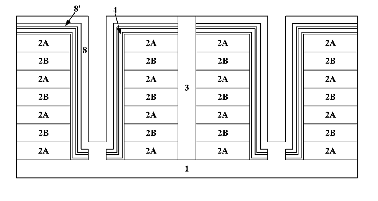
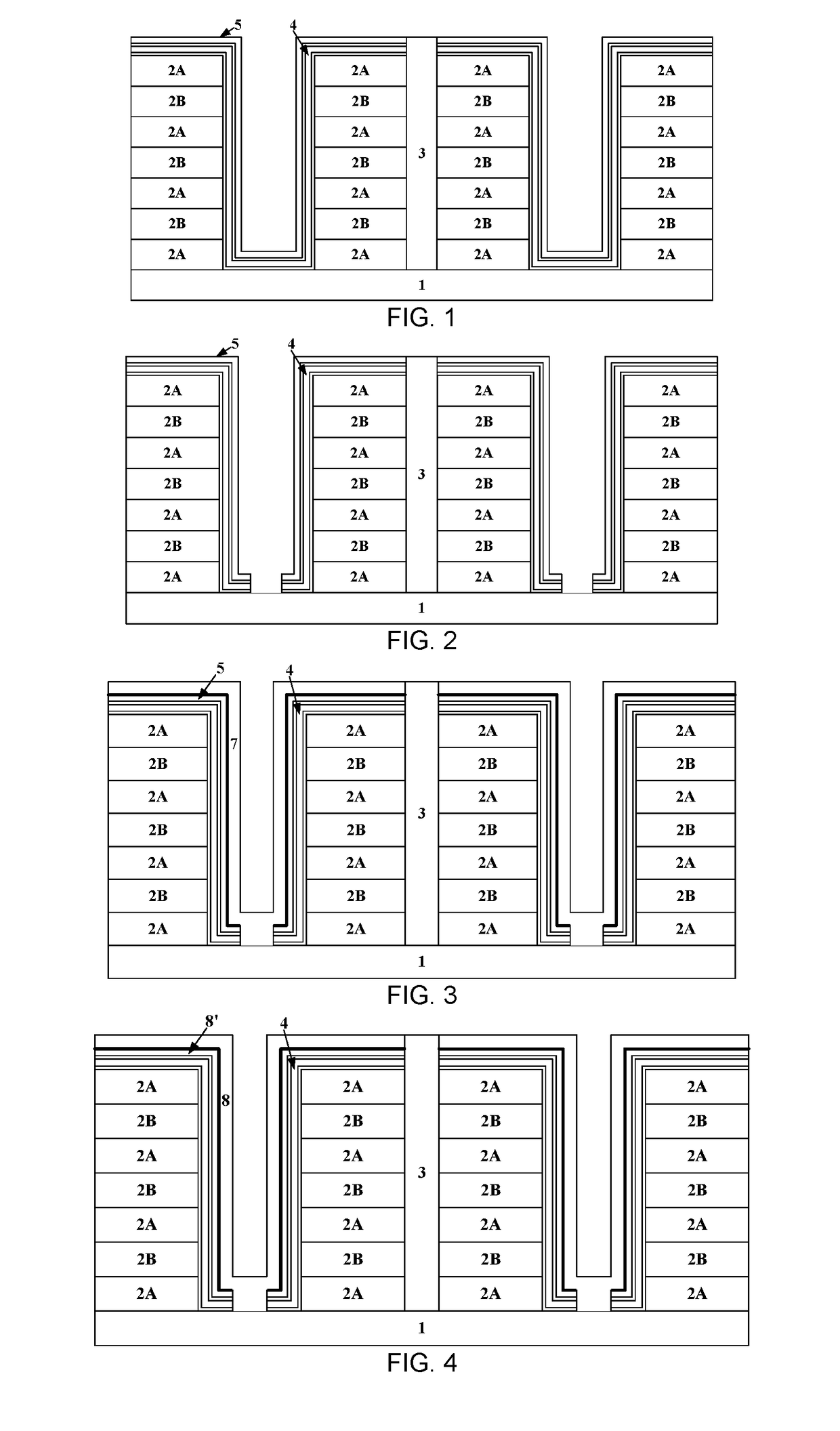
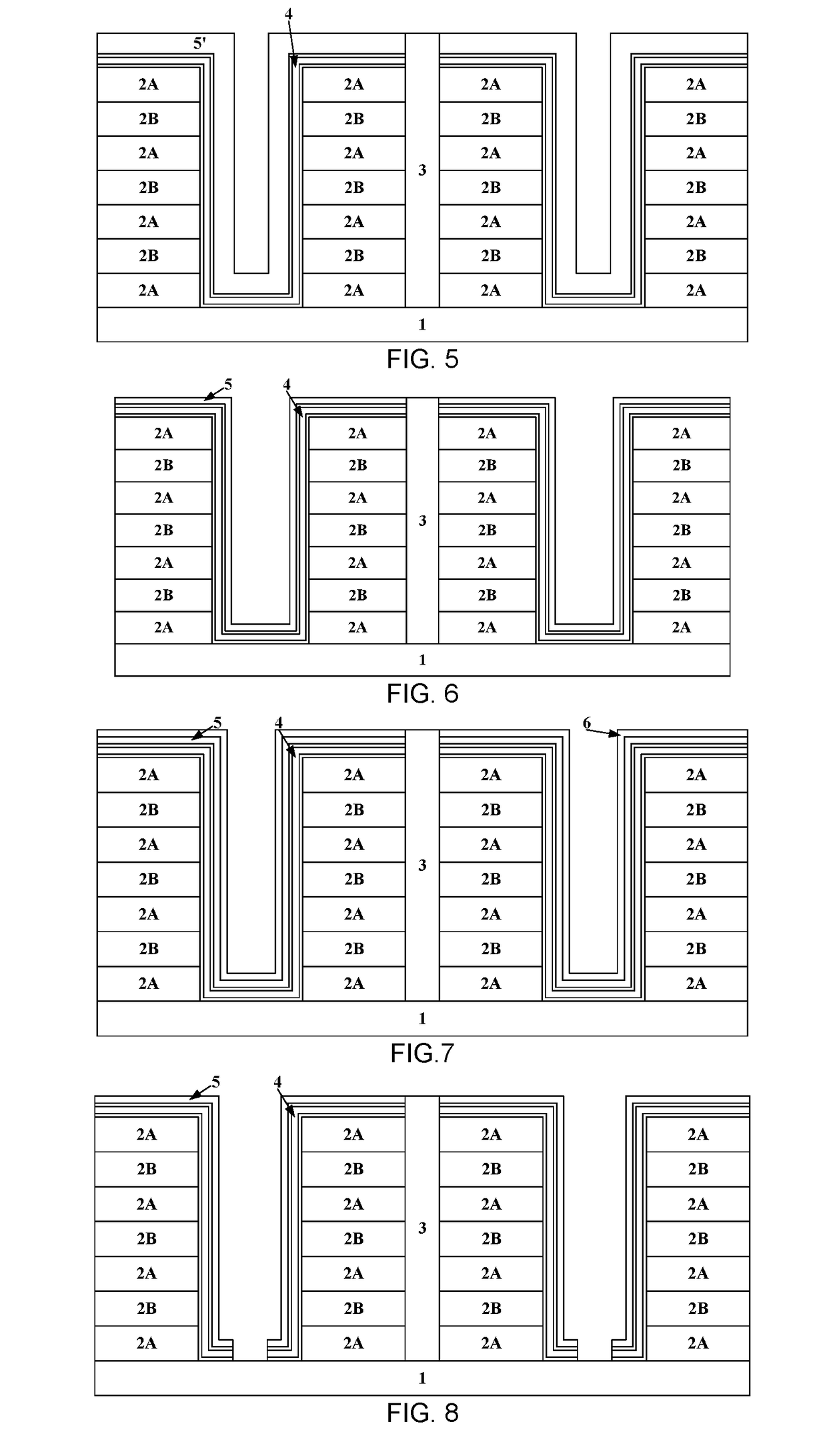
[0023]As shown in FIG. 12 and FIG. 5, a gate dielectric layer 4 and a first amorphous channel layer 5′ are formed in a plurality of channel trenches on a substrate 1.

[0024]A stacked structure 2 alternately composed of a plurality of first material layers 2A and a plurality of second material layers 2B is formed on the substrate 1. ...


PUM

PropertyMeasurementUnit
thicknessaaaaaaaaaa
temperatureaaaaaaaaaa
thicknessaaaaaaaaaa

Abstract

A method of manufacturing a semiconductor device, comprising the steps of: forming a gate dielectric layer and a first amorphous channel layer on a substrate; thinning the first amorphous channel layer; etching the first amorphous channel layer and the gate dielectric layer until the substrate is exposed; forming a second amorphous channel layer on the first amorphous channel layer and the substrate; annealing such that the first amorphous channel layer and the second amorphous channel layer are converted into a polycrystalline channel layer; and thinning the polycrystalline channel layer. According to the method of manufacturing semiconductor device of the present invention, the grain size of the polycrystalline thin film is increased by depositing a thick amorphous film and then annealing and thinning it. An additional protective layer is used to avoid etching damage on the sidewalls, effectively reducing the interface state and damage defects of the polycrystalline channel layer, thereby enhancing the reliability of the device.

Description

TECHNICAL FIELD[0001]The present invention relates to a method of manufacturing a semiconductor device, particularly to a method of manufacturing a polycrystalline channel layer of three-dimensional memory.BACKGROUND[0002]In order to improve the density of memory device, the industry has worked extensively at developing a method for reducing the size of a two-dimensional arrangement of memory cells. As the size of the memory cells of two-dimensional (2D) memory devices continues to shrink, signal conflict and interference will significantly increase, so that it is difficult to perform operation of multi-level cell (MLC). In order to overcome the limitations of 2D memory devices, the industry has developed a memory device having a three-dimensional (3D) structure, to improve integration density by arranging the memory cells over the substrate three-dimensionally.[0003]Due to its special three-dimensional structure and complicated process inheritance, three-dimensional memory can only...

Claims


Application Information

Patent Timeline
Patent Type & Authority Applications(United States)
IPC IPC(8): H01L27/11582H01L21/02H01L21/306H01L21/324H01L21/28
CPCH01L27/11582H01L21/02592H01L21/02667H01L21/30604H01L21/324H01L21/28282H01L21/02532H01L21/02529H01L21/02527H01L21/02538H01L21/02551H01L29/7926H10B43/27H01L29/40117
Inventor YE, TIANCHUN
Owner INST OF MICROELECTRONICS CHINESE ACAD OF SCI
Why Eureka
Try Eureka