Method of processing wafer and protective sheeting for use in this method
- Summary
- Abstract
- Description
- Claims
- Application Information
AI Technical Summary
Benefits of technology
Problems solved by technology
Method used
Image
Examples
first embodiment
[0121]In the following, a method of processing a wafer W according to the present invention will be described with reference to FIGS. 1 to 11.
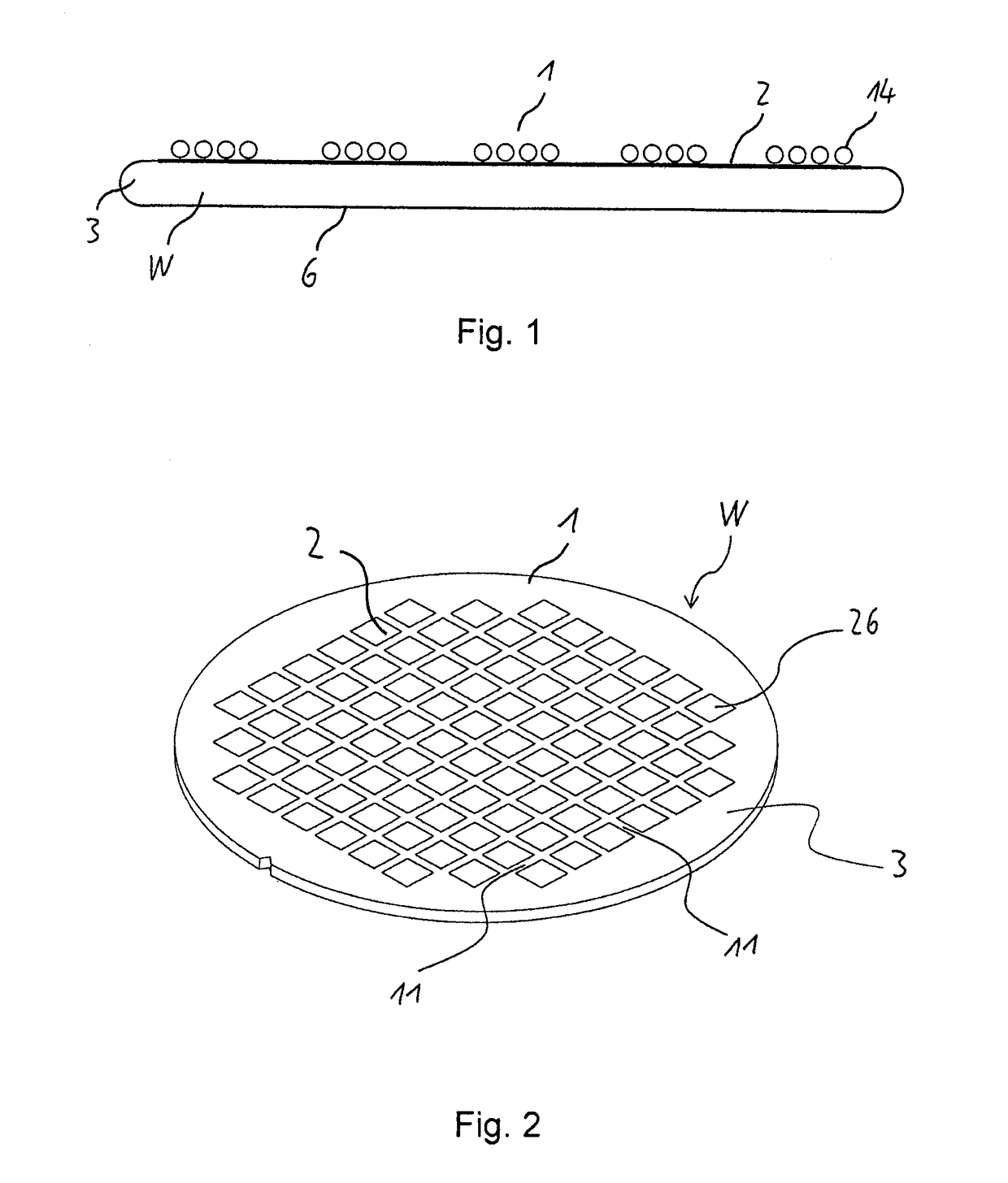
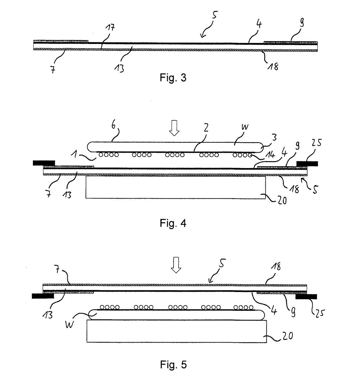
[0122]FIG. 1 shows a cross-sectional view of the wafer W to be processed by the method of the present invention. FIG. 2 shows a perspective view of the wafer W shown in cross-section in FIG. 1. FIG. 3 shows a cross-sectional view of a protective sheeting 5 according to a first embodiment of the present invention.
[0123]As is shown in FIG. 3, the protective sheeting 5 comprises a base sheet 7, a cushioning layer 13 applied to a front surface 17 of the base sheet 7, a protective film 4, a back surface of which is attached to the cushioning layer 13, and an adhesive layer 9 applied to a part of a front surface of the protective film 4 opposite to the back surface thereof. Specifically, the adhesive layer 9 has an annular shape and is provided in a circumferential or peripheral portion of the front surface of the protective film 4.
[0124]Alternative...
second embodiment
[0160]In the following, a method of processing a wafer W according to the present invention will be described with reference to FIGS. 12 to 15.
[0161]The method of the second embodiment substantially differs from the method of the first embodiment in that no annular frame, such as the annular frame 25 shown in FIGS. 4 to 6, is used. The processing method of this second embodiment employs a protective sheeting 5′ according to a second embodiment of the present invention (see FIG. 12) which differs from the protective sheeting 5 according to the first embodiment in that it has a smaller outer diameter.
[0162]Specifically, as is schematically shown in FIG. 13, the outer diameter of the protective sheeting 5′ is only slightly larger, e.g., by 0.5 to 2.0 mm, than the outer diameter of the wafer W.
[0163]Alternatively, the outer diameter of the protective sheeting 5′ may be substantially the same as the outer diameter of the wafer W.
[0164]Otherwise, the processing steps shown in FIGS. 13 to ...
PUM
 Abstract
Description
Claims
Application Information


