Method of fabricating surface-emitting laser

a surface-emitting laser and laser technology, applied in the direction of laser details, semiconductor/solid-state device testing/measurement, lasers, etc., can solve the problems of increasing the difficulty in detecting and not easy to detect the etching end poin

Inactive Publication Date: 2018-10-04
SUMITOMO ELECTRIC IND LTD
View PDF2 Cites 3 Cited by
  • Summary
  • Abstract
  • Description
  • Claims
  • Application Information

AI Technical Summary

Benefits of technology

[0006]These and other objects, features, and advantages of the present invention will be more easily clarified from the following detailed description of a preferred embodiment of the present invention described with reference to the accompanying drawings.

Problems solved by technology

It is not easy to detect the etching end point when a stacked semiconductor layer having such a complex structure is etched.
This further increases the difficulty in detecting the etching end point.

Method used


Image

  • Method of fabricating surface-emitting laser
  • Method of fabricating surface-emitting laser
  • Method of fabricating surface-emitting laser

Examples


example

[0055]A time period for observing photoluminescence P1: 18 seconds[0056]A time period after losing the photoluminescence P1 before start of the etching of the lower contact layer: 30 seconds

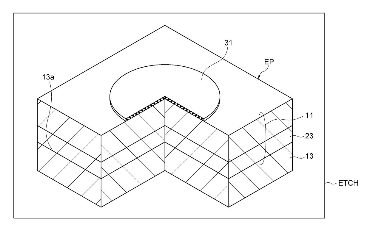
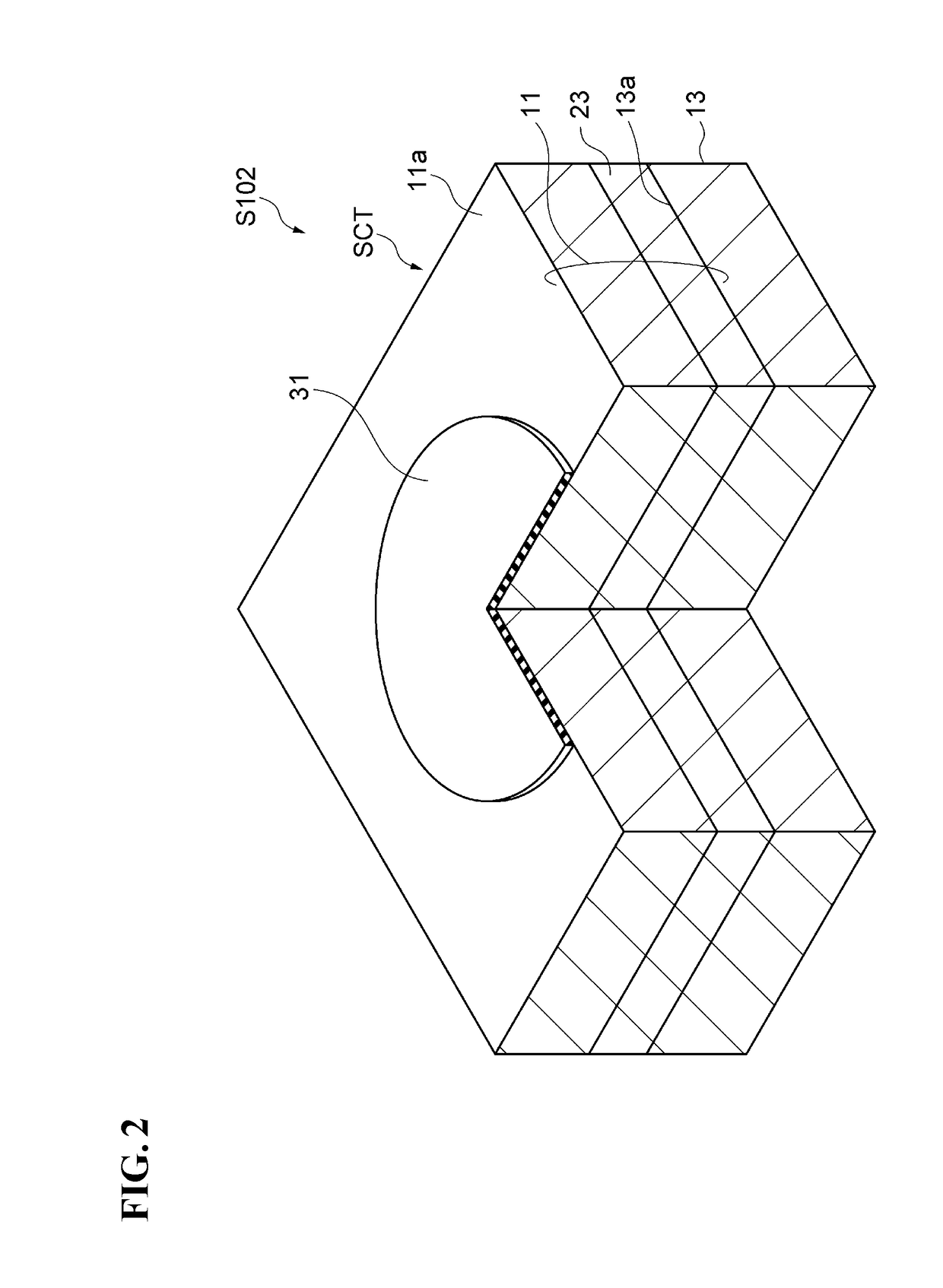
[0057]The end point detection may be determined after waiting for an elapse of time from detection of the photoluminescence P1. Specifically, the end point is determined with reference to a peak of the intensity of the optical spectrum in the measurement of photoluminescence. According to this method of fabricating, when the residual film of the upper stacked semiconductor layer is substantially eliminated, the optical confinement effect of the upper stacked semiconductor layer is also lost, and the strong photoluminescence from the active layer is temporarily observed before start of the etching of the active layer.

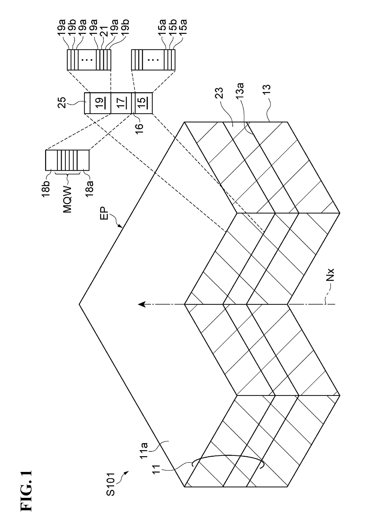
[0058]Meanwhile, the interference end point monitor utilizes the fact that the first stacked semiconductor layer 15 includes an AlGaAs / AlGaAs multi-layer and the substrate 13 includes...


PUM


Abstract

A method of fabricating a surface-emitting laser includes the steps of preparing an epitaxial substrate that includes an active layer and an upper stacked semiconductor layer provided on the active layer, the upper stacked semiconductor layer including a structure for forming an upper distributed Bragg reflector; forming a mask for forming a semiconductor post on the epitaxial substrate; and etching the epitaxial substrate by dry etching using the mask. The step of etching the epitaxial substrate includes the steps of measuring photoluminescence from the epitaxial substrate in response to excitation light during the etching so as to monitor an end point of the dry etching in accordance with a result of the measuring; and ending the dry etching in response to detection of the end point.

Description

BACKGROUND OF THE INVENTION1. Field of the Invention[0001]The present invention relates to a method of fabricating surface-emitting lasers.2. Description of the Related Art[0002]Patent Literature 1 (Japanese Patent No. 5034662) discloses a method of fabricating a surface-emitting laser.SUMMARY OF THE INVENTION[0003]In order to fabricate a post structure of a vertical cavity surface-emitting laser (VCSEL), a thick stacked semiconductor layer needs to be etched. In the VCSEL, the stacked semiconductor layer includes two distributed Bragg reflectors and an active layer disposed between the distributed Bragg reflectors. An end point of the etching relates to the height of the post structure. The post structure defines an optical resonator of the VCSEL. The height of the post structure is one of the most important parameters for designing the optical resonator of the VCSEL. In a process of etching the stacked semiconductor layer, detection of an appropriate end point is important for obt...

Claims


Application Information

Patent Timeline
Patent Type & Authority Applications(United States)
IPC IPC(8): H01S5/183H01S5/026
CPCH01S5/183H01S5/026H01S5/0042H01S5/18344H01S5/18347H01S5/3432H01S5/2086H01L22/12H01L22/26
Inventor TSUJI, YUKIHIRO
Owner SUMITOMO ELECTRIC IND LTD
Why Eureka
Try Eureka