Contour based defect detection

a technology of contour and defect detection, applied in the direction of image enhancement, semiconductor/solid-state device testing/measurement, instruments, etc., can solve the problems of not being able to quantify the hot spots of the image, requiring parameter tweaking, and unable to meet the requirements of imaging conditions

Active Publication Date: 2018-10-11
KLA TENCOR TECH CORP
View PDF1 Cites 87 Cited by
  • Summary
  • Abstract
  • Description
  • Claims
  • Application Information

AI Technical Summary

Problems solved by technology

However, as the dimensions of semiconductor devices decrease, inspection becomes even more important to the successful manufacture of acceptable semiconductor devices because smaller defects can cause the devices to fail.
Currently used methods for CD-SEMs have several challenges such as that they are slow, they require careful setup for each site and a knowledge of which sites to measure, and their results need to be interpreted further downline.
The main challenges of these previous attempts lie in heuristic determination of contours which can fail for complex patterns and pattern intersections.
These attempts also lack robustness to imaging conditions and require parameter tweaking for noisy and soft images.
However, none of these methods quantify these hot spots by reporting a CD metric which is required in order to accurately determine a hot spot based on the user-defined threshold.
For example, the currently used methods have no flexibility to automatically adapt to different pattern types (i.e., memory or logic).
In addition, the currently used methods have no generalization to different image modalities.
In a further example, the currently used methods provide no quantitative pattern characterization and hot spot detection.
In yet another example, the currently used methods provide no ability to handle OPC errors naturally without having to handle each kind of OPC error heuristically.

Method used


Image

  • Contour based defect detection
  • Contour based defect detection
  • Contour based defect detection

Examples


Embodiment Construction

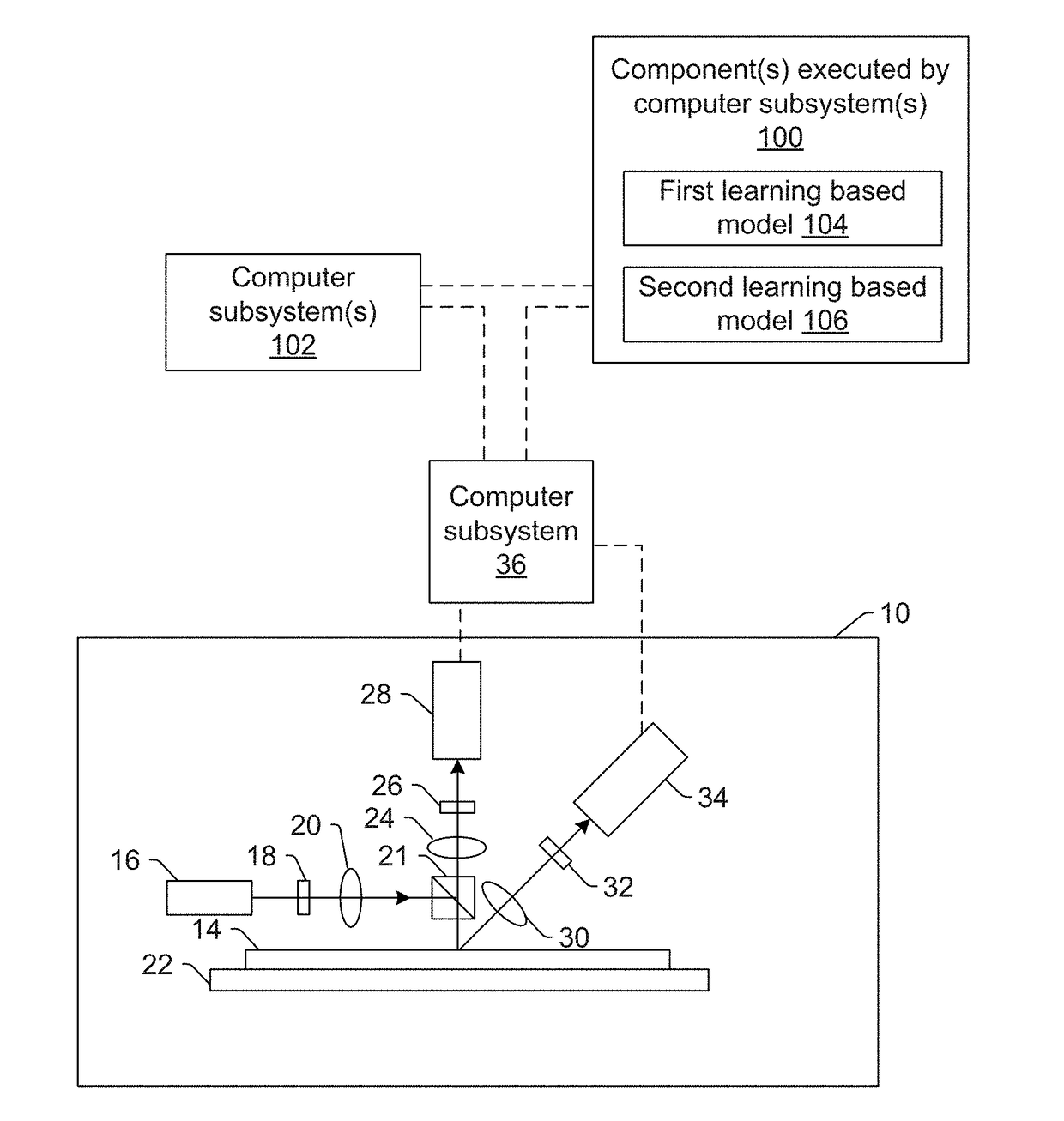
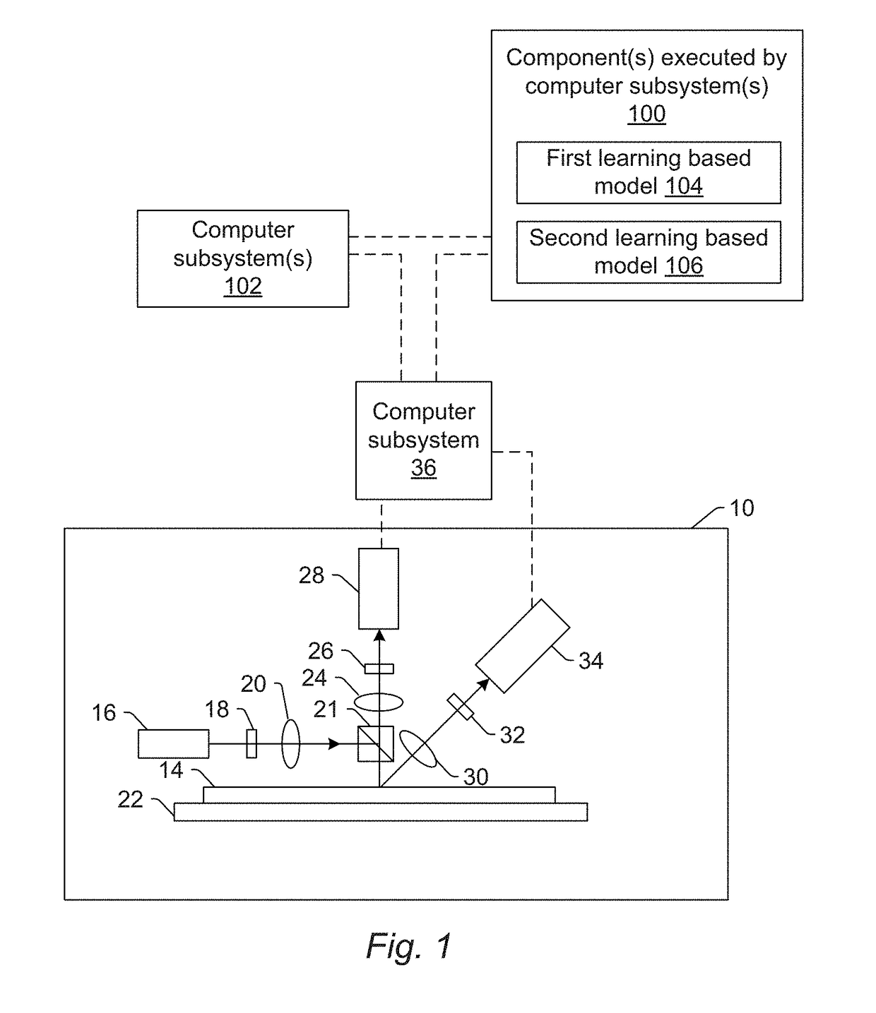
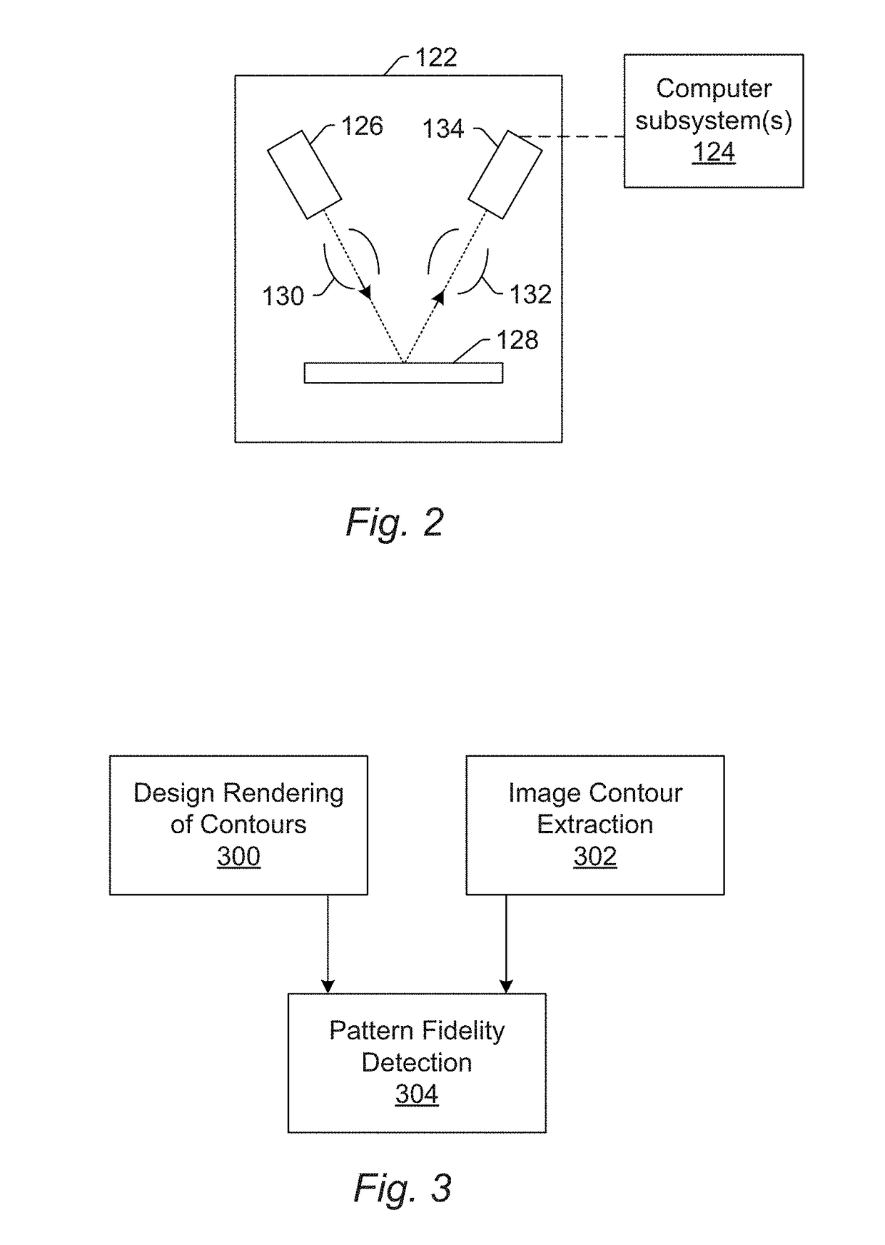
[0025]The terms “design” and “design data” as used herein generally refer to the physical design (layout) of an IC and data derived from the physical design through complex simulation or simple geometric and Boolean operations. The physical design may be stored in a data structure such as a graphical data stream (GDS) file, any other standard machine-readable file, any other suitable file known in the art, and a design database. A GDSII file is one of a class of files used for the representation of design layout data. Other examples of such files include GL1 and OASIS files and proprietary. file formats such as RDF data, which is proprietary to KLA-Tencor, Milpitas, Calif. In addition, an image of a reticle acquired by a reticle inspection system and / or derivatives thereof can be used as a “proxy” or “proxies” for the design. Such a reticle image or a derivative thereof can serve as a substitute for the design layout in any embodiments described herein that use a design. The design ...


PUM

PropertyMeasurementUnit
energyaaaaaaaaaa
densitiesaaaaaaaaaa
imaging parametersaaaaaaaaaa

Abstract

Methods and systems for detecting defects in patterns formed on a specimen are provided. One system includes one or more components executed by one or more computer subsystems, and the component(s) include first and second learning based models. The first learning based model generates simulated contours for the patterns based on a design for the specimen, and the simulated contours are expected contours of a defect free version of the patterns in images of the specimen generated by an imaging subsystem. The second learning based model is configured for generating actual contours for the patterns in at least one acquired image of the patterns formed on the specimen. The computer subsystem(s) are configured for comparing the actual contours to the simulated contours and detecting defects in the patterns formed on the specimen based on results of the comparing.

Description

BACKGROUND OF THE INVENTION1. Field of the Invention[0001]The present invention generally relates to methods and systems for detecting defects in patterns formed on a specimen.2. Description of the Related Art[0002]The following description and examples are not admitted to be prior art by virtue of their inclusion in this section.[0003]Inspection processes are used at various steps during a semiconductor manufacturing process to detect defects on wafers to drive higher yield in the manufacturing process and thus higher profits. Inspection has always been an important part of fabricating semiconductor devices. However, as the dimensions of semiconductor devices decrease, inspection becomes even more important to the successful manufacture of acceptable semiconductor devices because smaller defects can cause the devices to fail.[0004]Defect review typically involves re-detecting defects detected as such by an inspection process and generating additional information about the defects a...

Claims


Application Information

Patent Timeline
Patent Type & Authority Applications(United States)
IPC IPC(8): G06T7/00G06T7/564G01N21/95G01N21/956G01N21/88
CPCG06T7/001G06T7/564G01N21/9501G01N21/95607G01N21/8851G06T2207/30148G01N2021/8887G06T2207/10061G06T2207/20081G06T2207/20084G01N21/956G01N2021/8867H01L22/12H01L22/20G06N3/08G06N3/047G06N3/045G06T7/0002G06T7/13G06V10/44
Inventor GUPTA, AJAYMAHADEVAN, MOHANVENKATARAMAN, SANKARYANG, HEDONGKARSENTI, LAURENTCARMON, YAIRBULLKICH, NOGADANINO, UDY
Owner KLA TENCOR TECH CORP
Why Eureka
Try Eureka