Inductor and method for manufacturing the same

a technology a manufacturing method, applied in the field of a screen printing method, can solve the problems of increasing the hardness of the metal, cracking or delamination, and the limitation of increasing the thickness of the coil pattern through screen printing method, and achieve the effect of enhancing q characteristics and lowering the resistance of the coil

Active Publication Date: 2018-10-18
SAMSUNG ELECTRO MECHANICS CO LTD
View PDF10 Cites 2 Cited by
  • Summary
  • Abstract
  • Description
  • Claims
  • Application Information

AI Technical Summary

Benefits of technology

[0009]An aspect of the present disclosure may provide an inductor including one or more via(s) each having first and second conductive layers formed of heterogeneous metals, thus lowering resistance of a coil to enhance Q characteristics.
[0010]Another aspect of the present disclosure may provide an inductor in which a thickness of a second conductive layer, among first and second conductive layers of a via, is limited, to secure reliability of a connection between interlayer coils after the coils are connected.

Problems solved by technology

The coil pattern is manufactured through a screen printing method, but there is a limitation in increasing a thickness of the coil pattern through the screen printing method.
Also, in the case of forming a thick coil pattern on a ceramic layer, when a plurality of sheets are stacked, cracking or delamination may occur due to the presence of a step between a portion in which the coil pattern is formed and a portion in which a coil is not formed.
Here, the formation of vias using metal plating may lead to an increase in hardness of the metal, causing interlayer insulation distances to be nonuniform during stacking.
When interlayer insulation distances of coil patterns are not uniform, it is difficult to secure Q characteristics of an inductor.

Method used


Image

  • Inductor and method for manufacturing the same
  • Inductor and method for manufacturing the same
  • Inductor and method for manufacturing the same

Examples


Embodiment Construction

[0021]Exemplary embodiments in the present disclosure will now be described in detail with reference to the accompanying drawings.

[0022]Hereinafter, an inductor 100 according to another exemplary embodiment in the present disclosure will be described.

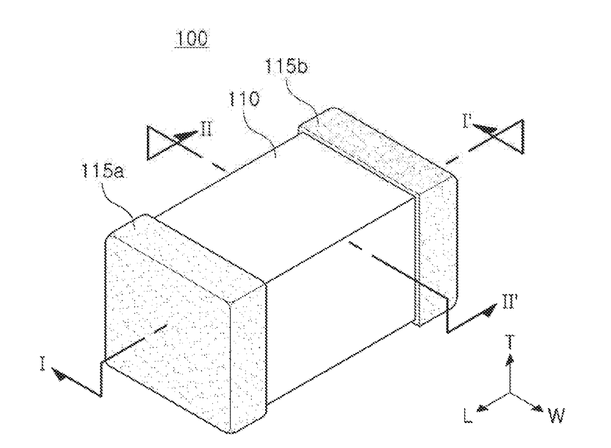
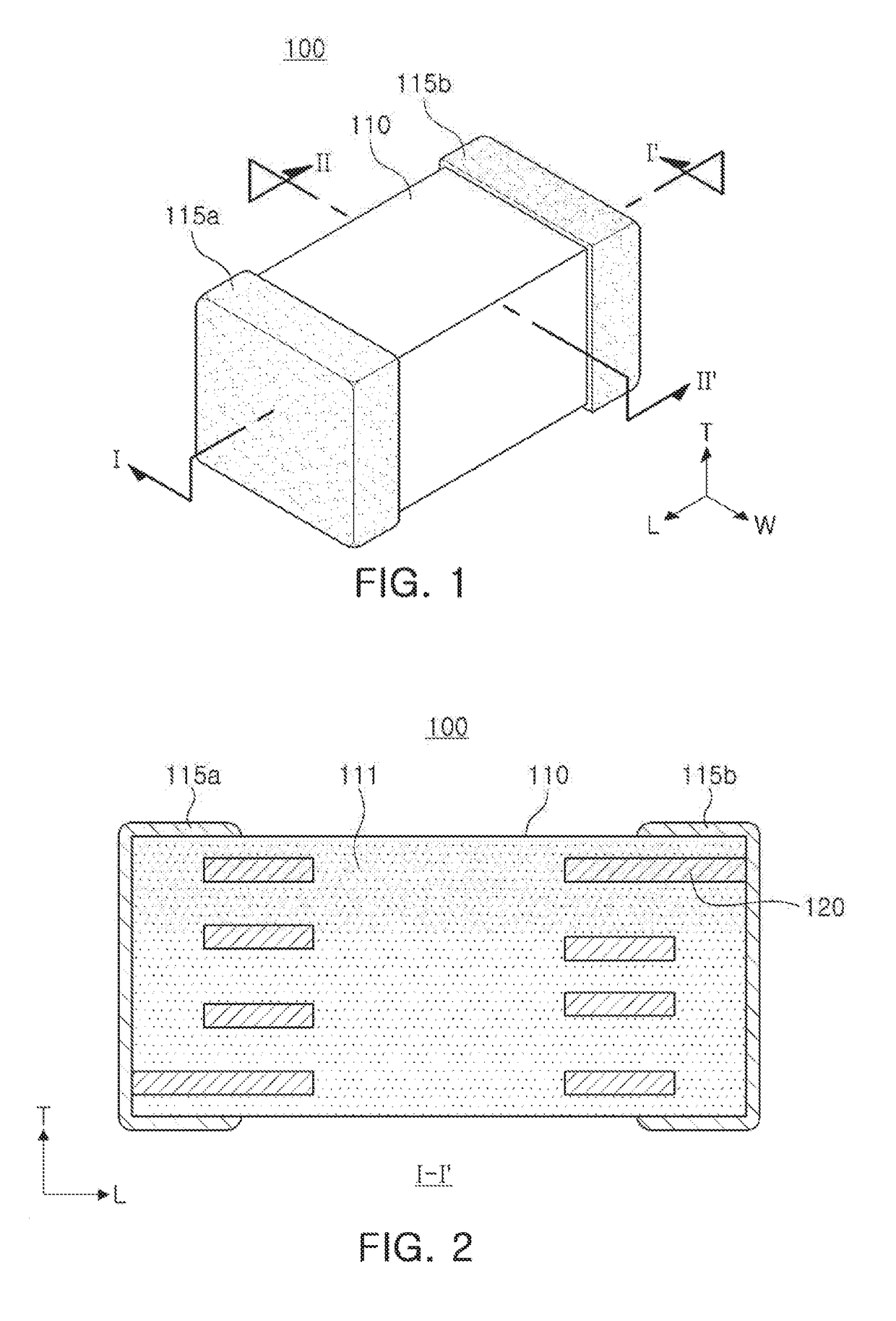
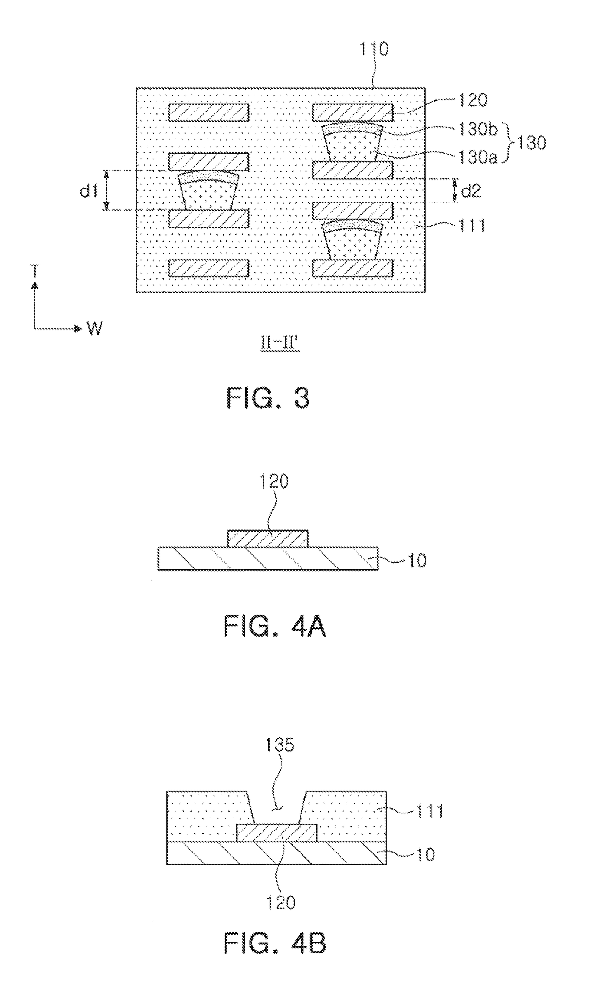
[0023]FIG. 1 is a schematic perspective view of an inductor according to an exemplary embodiment in the present disclosure, FIG. 2 is a schematic cross-sectional view of an inductor such as a view taken along line I-I′ in the inductor of FIG. 1 according to an exemplary embodiment in the present disclosure, and FIG. 3 is a schematic lateral cross-sectional view of an inductor such as a view taken along line II-II′ in the inductor of FIG. 1 according to an exemplary embodiment in the present disclosure.

[0024]Referring to FIGS. 1 to 3, the inductor 100 according to an exemplary embodiment in the present disclosure includes a body 110 in which a coil 120 formed as a plurality of coil patterns interconnected by vias 130 is disposed. Each vi...


PUM

PropertyMeasurementUnit
thicknessaaaaaaaaaa
frequencyaaaaaaaaaa
thicknessaaaaaaaaaa

Abstract

An inductor includes a body in which is disposed a coil formed as a plurality of coil patterns connected by one or more via(s). Each via includes a first conductive layer and a second conductive layer formed on the first conductive layer, and a distance between portions of coil patterns connected by the via in the body is greater than a distance between other portions of the coil patterns in the body. Methods of forming inductors having vias including first and second conductive layers are also provided.

Description

CROSS-REFERENCE TO RELATED APPLICATION(S)[0001]This application claims benefit of priority to Korean Patent Application No. 10-2017-0047310 filed on Apr. 12, 2017 in the Korean Intellectual Property Office, the disclosure of which is incorporated herein by reference in its entirety.BACKGROUND1. Field[0002]The present disclosure relates to an inductor and a method for manufacturing the same.2. Description of Related Art[0003]A general multilayer inductor has a structure in which a plurality of insulating layers each having a conductive pattern formed thereon are stacked, and in which the conductive patterns are sequentially connected by conductive vias formed in the respective insulating layers. The interconnected patterns thereby form a coil having a spiral structure. Both ends of the coil are led out to external surfaces of a multilayer body and connected to external terminals.[0004]An inductor is generally provided as a surface-mount device type that can be mounted on a circuit bo...

Claims


Application Information

Patent Timeline
Patent Type & Authority Applications(United States)
IPC IPC(8): H01F27/29H01F41/04H01F41/10
CPCH01F27/292H01F41/041H01F41/10H01F2005/006H01F17/0013H01F2017/002H01F2017/004H01F1/015H01F27/30H01F41/02
Inventor PAENG, SE WOONGBAE, JONG SEOKKIM, SOO YEOL
Owner SAMSUNG ELECTRO MECHANICS CO LTD
Why Eureka
Try Eureka