Unlock instant, AI-driven research and patent intelligence for your innovation.

Low temperature selective epitaxial silicon deposition

a silicon deposition and low temperature technology, applied in the direction of crystal growth process, polycrystalline material growth, chemically reactive gas, etc., can solve the problem of additional processing capacity demands

Inactive Publication Date: 2018-10-25
APPLIED MATERIALS INC
View PDF0 Cites 2 Cited by
  • Summary
  • Abstract
  • Description
  • Claims
  • Application Information

AI Technical Summary

Benefits of technology

This patent describes a method for making semiconductor devices using a self-assembled monolayer (SAM) to selectively deposit materials on different materials on a substrate. The method involves exposing the substrate to a SAM forming molecule, such as a chlorosilane molecule, to selectively deposit a SAM film on the exposed dielectric material while removing the SAM film from the exposed silicon material. Then, a silicon-containing material layer is selectively deposited on the exposed silicon material. This method can be performed at a low temperature and allows for precise deposition of materials without damaging the substrate.

Problems solved by technology

Reliably producing sub-half micron and smaller features is one of the key technology challenges for next generation very-large-scale integration (VLSI) and ultra-large-scale integration (ULSI) of semiconductor devices.
However, as the limits of circuit technology are pushed, the shrinking dimensions of VLSI and ULSI technology have placed additional demands on processing capabilities.

Method used


Image

  • Low temperature selective epitaxial silicon deposition
  • Low temperature selective epitaxial silicon deposition
  • Low temperature selective epitaxial silicon deposition

Examples


Embodiment Construction

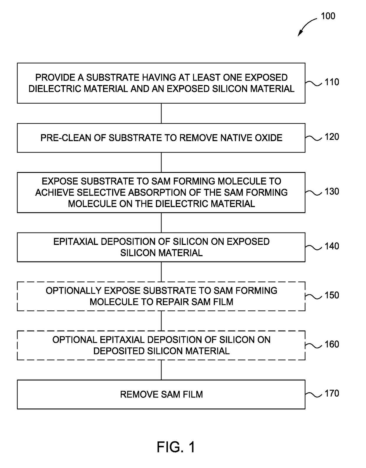
[0013]The following disclosure describes processes for the fabrication of semiconductor devices in which a self-assembled monolayer is used to achieve selective deposition at lower temperatures. Certain details are set forth in the following description and in FIGS. 1-2G to provide a thorough understanding of various implementations of the disclosure. Other details describing well-known structures and systems often associated with semiconductor devices, self-assembled monolayers, epitaxial deposition and surface preparation are not set forth in the following disclosure to avoid unnecessarily obscuring the description of the various implementations.

[0014]Many of the details, dimensions, angles and other features shown in the Figures are merely illustrative of particular implementations. Accordingly, other implementations can have other details, components, dimensions, angles and features without departing from the spirit or scope of the present disclosure. In addition, further implem...


PUM

PropertyMeasurementUnit
Temperatureaaaaaaaaaa

Abstract

Implementations described herein generally relate to processes for the fabrication of semiconductor devices in which a self-assembled monolayer (“SAM”) is used to achieve selective epitaxial deposition. In one implementation, a method of processing a substrate is provided. The method comprises exposing a substrate to a self-assembled monolayer (“SAM”) forming molecule to selectively deposit a SAM film on an exposed dielectric material, wherein the substrate comprises the exposed dielectric material and an exposed silicon material. The SAM forming molecule is a chlorosilane molecule. The method further comprises epitaxially and selectively depositing a silicon-containing material layer on the exposed silicon material at a temperature of 400 degrees Celsius or lower. The method further comprises removing the SAM film from the exposed dielectric material.

Description

CROSS-REFERENCE TO RELATED APPLICATIONS[0001]This application claims benefit of U.S. Provisional Patent Application Ser. No. 62 / 488,360, filed Apr. 21, 2017, which is incorporated herein by reference in its entirety.BACKGROUNDField[0002]Implementations described herein generally relate to processes for the fabrication of semiconductor devices in which a self-assembled monolayer (“SAM”) is used to achieve selective epitaxial deposition.Description of the Related Art[0003]Reliably producing sub-half micron and smaller features is one of the key technology challenges for next generation very-large-scale integration (VLSI) and ultra-large-scale integration (ULSI) of semiconductor devices. However, as the limits of circuit technology are pushed, the shrinking dimensions of VLSI and ULSI technology have placed additional demands on processing capabilities. Reliable formation of gate structures on substrates is a component of VLSI and ULSI success and to the continued effort to increase ci...

Claims


Application Information

Patent Timeline
IPC IPC(8): H01L21/02C23C16/24C23C16/455C30B25/02C30B29/06
CPCC23C16/45553C30B25/02C30B29/06H01L21/02381H01L21/0262H01L21/02532C23C16/24H01L21/02642C23C16/0272C23C16/04
Inventor BAJAJ, GEETIKAGORADIA, PRERNA SONTHALIAVISSER, ROBERT JAN
Owner APPLIED MATERIALS INC
Features
  • R&D
  • Intellectual Property
  • Life Sciences
  • Materials
  • Tech Scout
  • Unparalleled Data Quality
  • Higher Quality Content
  • 60% Fewer Hallucinations
Learn More