Touch device and touch display panel

a touch display panel and touch technology, applied in the field of touch devices and touch display panels, can solve the problem of insufficient sensing signal intensity, and achieve the effect of reducing the capacitance between the patterned sensing electrode structure and the patterned common electrode layer

Active Publication Date: 2018-11-08
AU OPTRONICS CORP
View PDF10 Cites 5 Cited by
  • Summary
  • Abstract
  • Description
  • Claims
  • Application Information

AI Technical Summary

Benefits of technology

[0005]It is therefore an objective of the present invention to provide a touch device and a touch display panel so as to reduce a coupling capacitance between a sensing electrode and a common electrode to increase intensity of a sensing signal.
[0026]The present invention provides the patterned sensing electrode structure corresponding to the light-shielding region combined with the electrode portions of the patterned common electrode layer, and reduces the area of the connecting portions, so that the overlap between the patterned sensing electrode structure and the patterned common electrode layer can be reduced. The coupling capacitance between the patterned sensing electrode structure and the patterned common electrode layer can therefore be reduced, and the intensity of the sensing signal sensed from the patterned sensing electrode structure can be increased accordingly.

Problems solved by technology

Therefore, the sensing pads are affected by the coupling capacitor when a finger touches the conventional touch display panel, and a problem of insufficient intensity of the sensing signal occurs.

Method used


Image

  • Touch device and touch display panel
  • Touch device and touch display panel
  • Touch device and touch display panel

Examples


Embodiment Construction

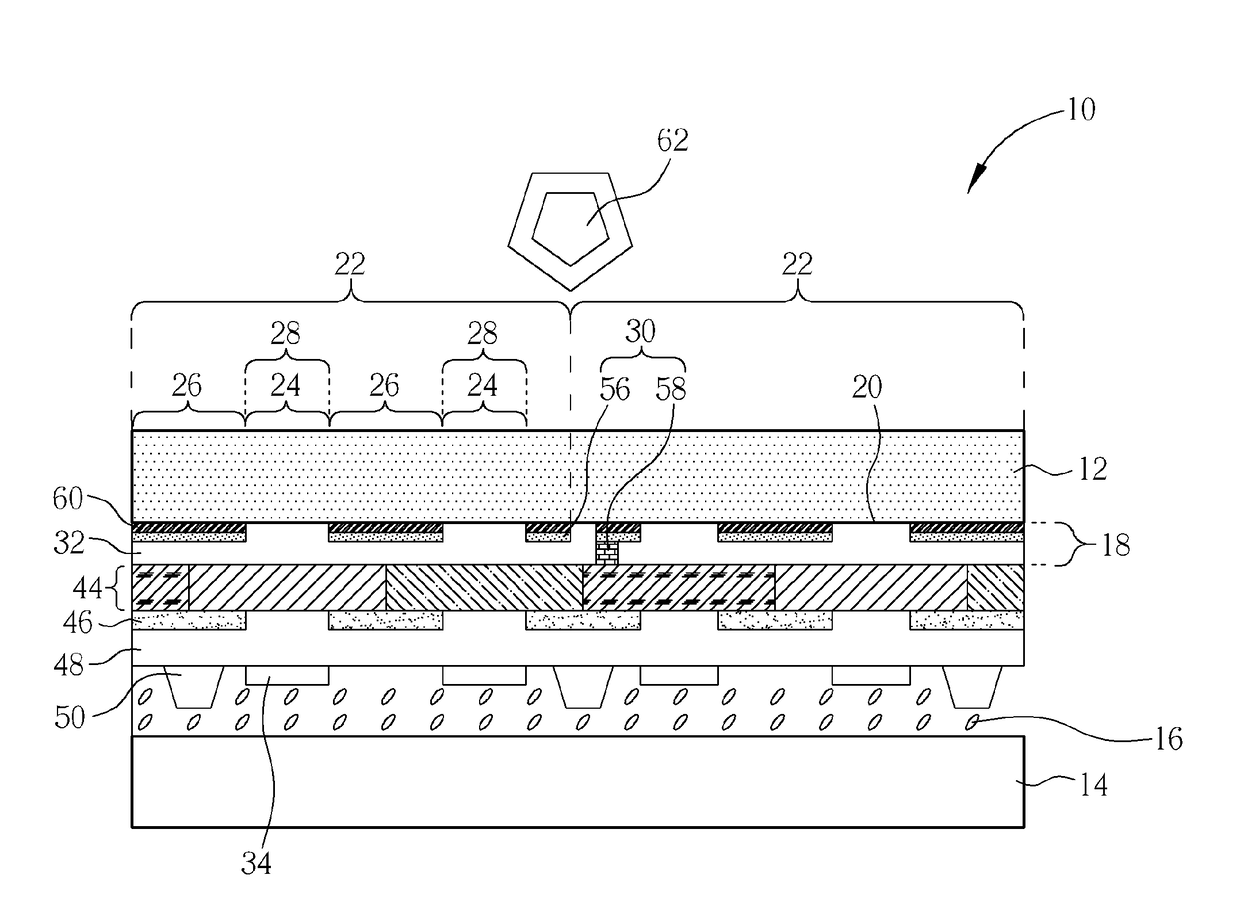
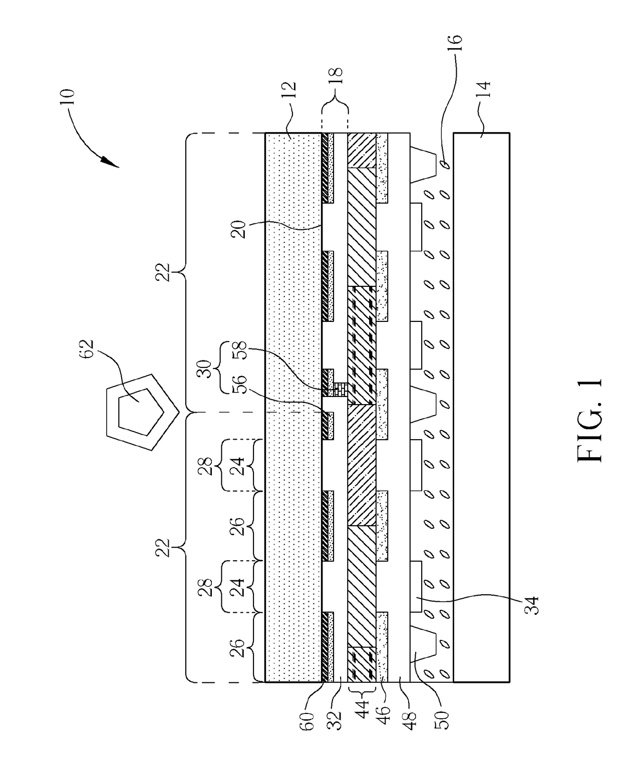
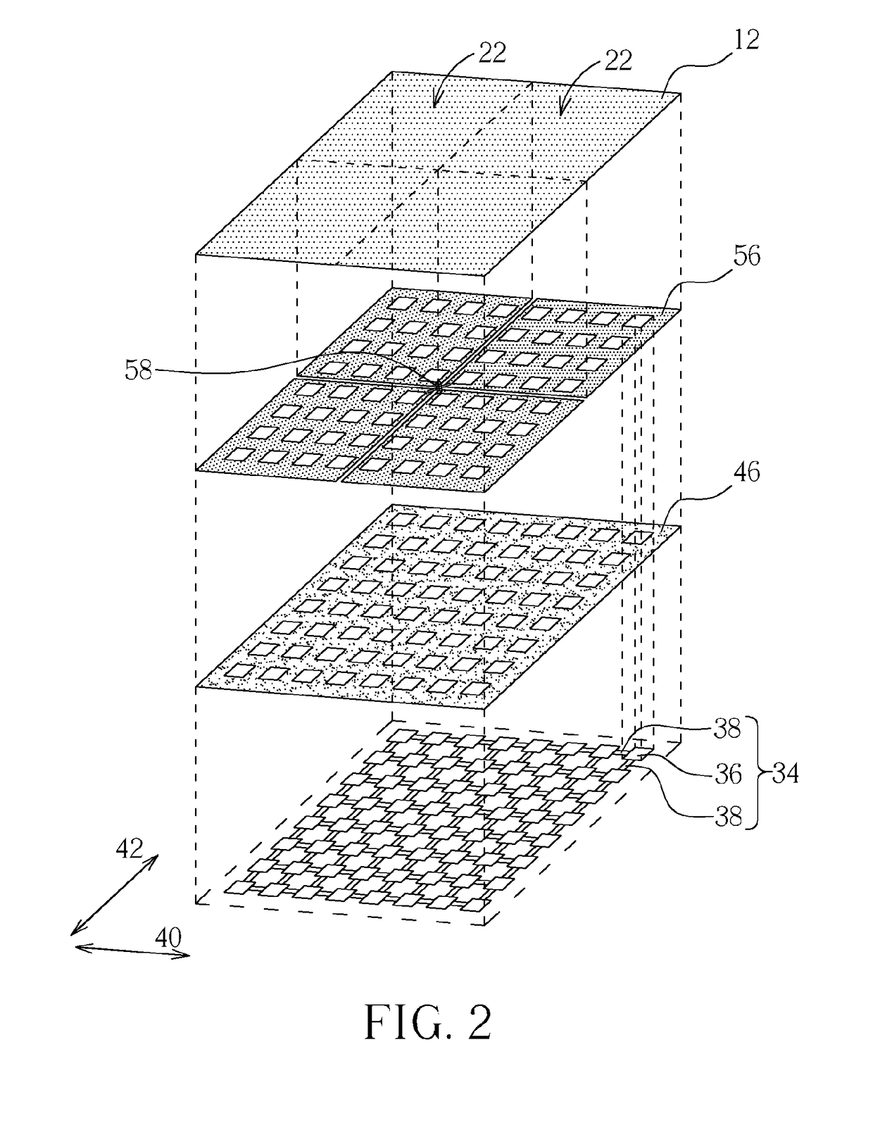
[0035]Referring to FIG. 1 and FIG. 2, FIG. 1 is a schematic diagram illustrating a cross-sectional structure of a touch display panel according to a first preferred embodiment of the present invention, and FIG. 2 is a schematic diagram illustrating the touch display panel according to the first preferred embodiment of the present invention. As shown in FIG. 1 and FIG. 2, the touch panel 10 includes a first substrate 12, a second substrate 14, a liquid crystal layer 16, and a touch device 18. The first substrate 12 and the second substrate 14 are parallel to each other, and the first substrate 12 has a surface 20 facing the second substrate 14. The surface 20 of the substrate 12 defines a plurality of sensing regions 22, and each sensing region 22 defines a plurality of displaying regions 24 arranged as a matrix formation and a light-shielding region 26 disposed between the displaying regions 24. The first substrate 12 can be a transparent substrate, such as glass substrate, quartz s...


PUM


Abstract

A touch display panel comprises a first substrate, a plurality of first sensing series and a plurality of second sensing series, wherein both the first sensing series and the second sensing series are above the first substrate, and the first sensing series and the second sensing series are crossly arranged to form a plurality of sensing series openings in between, a first insulating layer, covering the first sensing series and the second sensing series, a patterned black matrix layer, comprising a plurality of black matrix openings arranged in a matrix formation, a second insulating layer, covering the patterned black matrix layer; and a patterned common electrodes layer. The plurality of sensing series openings, the plurality of black matrix openings, and the patterned common electrode layer are overlapped.

Description

CLAIM OF PRIORITY[0001]This application is a continuation in part of U.S. patent application Ser. No. 14 / 884,769, which is a continuation of U.S. patent application Ser. No. 12 / 434,681, which claims foreign priority to Taiwanese Patent Application No. 097148203 filed Dec. 11, 2008.FIELD OF THE INVENTION[0002]The present invention relates to a touch device and a touch display panel.DESCRIPTION OF THE PRIOR ART[0003]LCD (liquid crystal display) is one type of flat display, popular on the market for its characteristics of power saving, thinness, and light weight. In any kind of electronic device that includes an LCD, such as a media player, mobile phone or personal digital assistant (PDA), a touch input function of the LCD is becoming more popular, with the result that touch panels are now in widespread use.[0004]Conventional touch display panels are mainly classified into resistance-type touch display panels and capacitor-type touch display panels. The resistance-type touch display pa...

Claims


Application Information

Patent Timeline
Patent Type & Authority Applications(United States)
IPC IPC(8): G06F3/044G09G3/36G06F3/041
CPCG09G3/36G06F2203/04112G06F2203/04111G06F3/0416G06F3/044G06F3/0412G06F2203/04106G02F1/13338G02F1/133512G06F3/0443G06F3/0446G02F1/134318
Inventor YANG, TUN-CHUNLEE, SEOK-LYULHUANG, WEI-MING
Owner AU OPTRONICS CORP
Why Eureka
Try Eureka