
Eureka
For R&D, Eureka makes reading and utilizing patents & technical documents easy.
Eureka AIR
Designed for self-driven R&D workflows. Generate viable solutions, solve complex R&D challenges, empower your innovation with AI.

Eureka Materials
Designed for material experts only. Revolutionize your material R&D, from search, analyze, to developing new materials.

TechResearch
Generate reliable direction feasibility study reports for your R&D in just a few steps.

TechSeek
Discover and master advanced knowledge NOW. Basics, ideas, possibilities, all at once.

TechMind
As an expert in R&D Theories, TechMind can generates customized viable solutions instantly.

TechRisk
Analyze your overall solution with one click, know your potential R&D risks in advance.

TechMonitor
Get weekly tech updates, stay abreast of the latest tech innovations and key insights.
Print head substrate and method of manufacturing the same, and semiconductor substrate
- Summary
- Abstract
- Description
- Claims
- Application Information
AI Technical Summary
Benefits of technology
Problems solved by technology
Method used
Image

Examples
embodiment 1
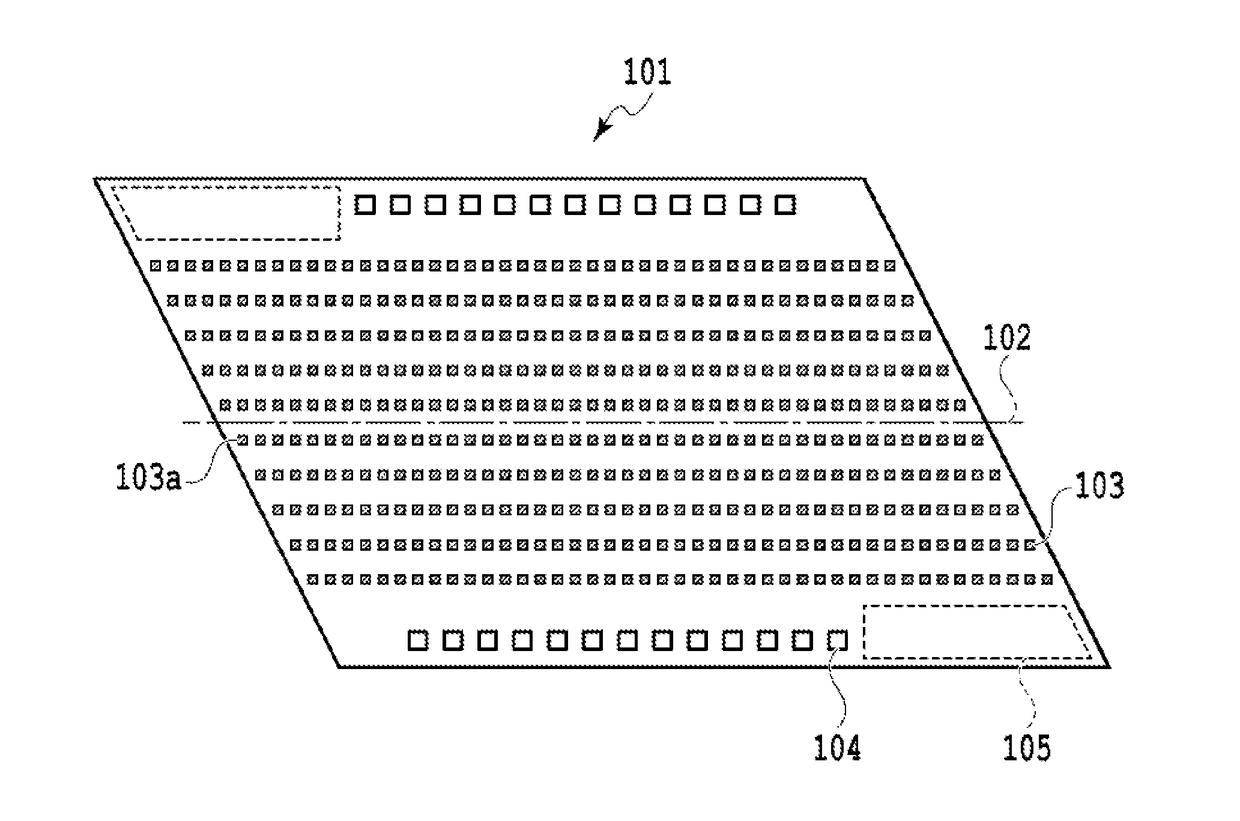
[0018]FIG. 1 is a diagram illustrating a print head substrate 101 of this embodiment. Multiple print head substrates 101 are arrayed to constitute a long-length print head (FIG. 9B). The print head substrate 101 has a parallelogram shape. The print head substrate 101 is a semiconductor chip. The print head substrate 101 cut out in the shape as illustrated in FIG. 1 is obtained by forming patterns of local work-affected layers with laser light focused inside a wafer substrate and cleaving the substrate along the formed patterns. In this way, the shape of the print head substrate 101 is formed by dicing called stealth dicing. In the print head substrate 101 of FIG. 1, two corners in FIG. 1, the lower-right corner and the upper-left corner, are acute angle portions.
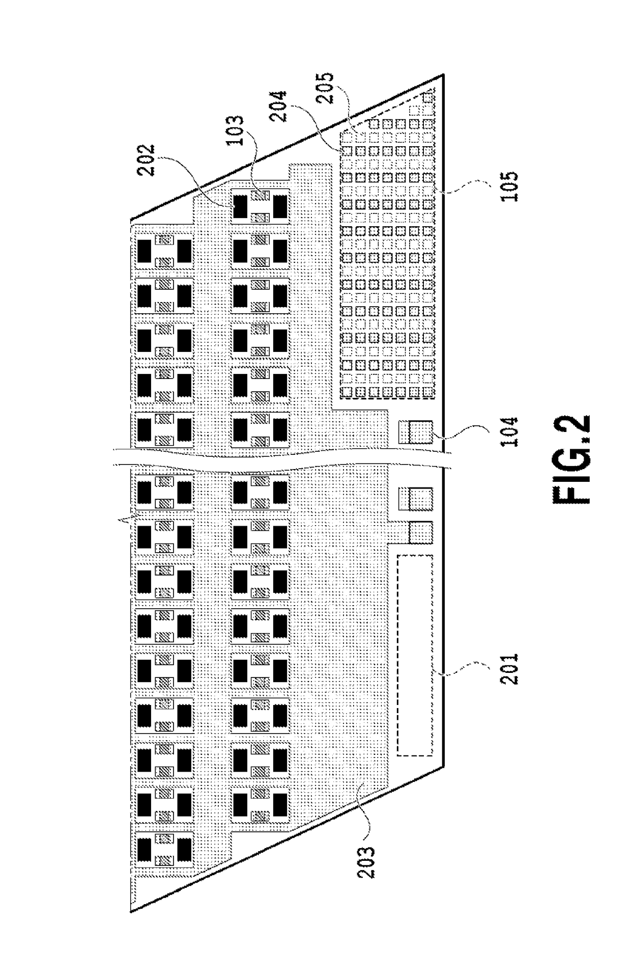
[0019]On the print head substrate 101, heaters 103 are lined up in multiple rows in an array shape. The heaters 103 are printing elements for ejecting ink for printing. In other words, the heaters 103 are heating elements fo...
embodiment 2
[0037]Descriptions have been provided for embodiment 1, using the case where the shape of the print head substrate is a parallelogram, as an example. In this embodiment, descriptions will be provided using the case where the shape of a print head substrate is a trapezoid, as an example.
[0038]FIG. 5 shows a trapezoidal print head substrate 501 in this embodiment. On the print head substrate 501, the PADs 104 are lined up along the longest side. This longest side forms acute angle portions. The TEG areas 105 are disposed on both the acute angle portion sides of the print head substrate 501. The print head substrate 501 does not have a chip separation border line 102 as in FIG. 1 and has the PADs 104 arrayed along one side of the substrate. The PADs 104 and the heaters 103 are disposed symmetrically. Although not illustrated, the power is supplied to the heaters 103 in each row with the same Al wiring trace as in FIGS. 2 and 3 of Embodiment 1. In the substrate shape and the heater arra...
embodiment 3
[0040]In Embodiment 3, descriptions will be provided for a print head substrate in which a moisture-resistant ring is formed. A moisture-resistant ring is a member commonly used in a semiconductor substrate using a planarization process such as chemical mechanical polishing (CMP). The moisture-resistant ring serves as a wall for protecting devices in the chip against the moisture from the chip cutting wall surfaces.
[0041]FIG. 6 illustrates the pattern of a moisture-resistant ring 602 in this embodiment. It is assumed that a print head substrate 601 has the same configuration as that of the print head substrate 101 described in Embodiment 1 except that the moisture-resistant ring 602 is formed in the print head substrate 601. As described in FIG. 6, the print head substrate 601 of this embodiment has a configuration in which a drive circuit area including the PADs 104 and wiring traces and TEG areas 105 are separated by the moisture-resistant ring 602. Specifically, in the print head...
PUM
 Abstract
Description
Claims
Application Information
 - R&D Engineer
- R&D Manager
- IP Professional
- Industry Leading Data Capabilities
- Powerful AI technology
- Patent DNA Extraction
Browse by: Latest US Patents, China's latest patents, Technical Efficacy Thesaurus, Application Domain, Technology Topic, Popular Technical Reports.
© 2024 PatSnap. All rights reserved.Legal|Privacy policy|Modern Slavery Act Transparency Statement|Sitemap|About US| Contact US: help@patsnap.com