Eureka AIR delivers breakthrough ideas for toughest innovation challenges, trusted by R&D personnel around the world.

Semiconductor device and manufacture thereof

Active Publication Date: 2018-11-22
SEMICON MFG INT (SHANGHAI) CORP +1
View PDF3 Cites 0 Cited by
  • Summary
  • Abstract
  • Description
  • Claims
  • Application Information

AI Technical Summary

Benefits of technology

The patent text describes a method for creating a groove in a semiconductor device by etching the insulation layer and a portion of the interlayer dielectric layer underneath it. This groove will expose a portion of the first metal layer. The technical effect of this process is to provide a better understanding of the metal layer's electrical properties and to facilitate the formation of additional layers during semiconductor device manufacturing.

Problems solved by technology

The manufacture of Backside Illuminated Complementary Metal-Oxide-Semiconductor Image Sensor (BSI CIS) is a complicated process.
In conventional manufacturing methods such as the one described above, the etching process conducted on the aluminum layer may leave some aluminum residues on the side surface of the opening, these aluminum residues may peel off and cause defects or even form a short circuit in the device in succeeding steps.
This method, however, may inadvertently damage the remaining aluminum layer, especially the side surface of the remaining aluminum layer, on the silicon layer.

Method used


Image

  • Semiconductor device and manufacture thereof
  • Semiconductor device and manufacture thereof
  • Semiconductor device and manufacture thereof

Examples


Embodiment Construction

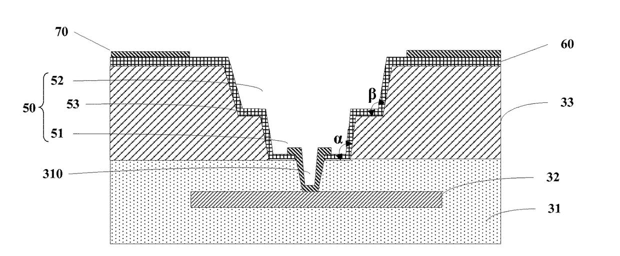
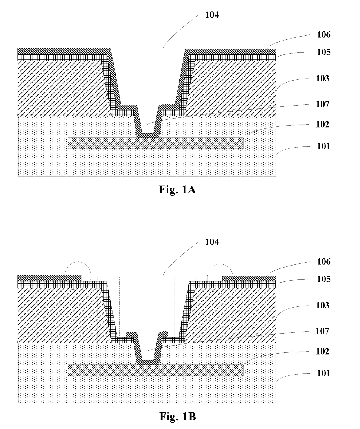
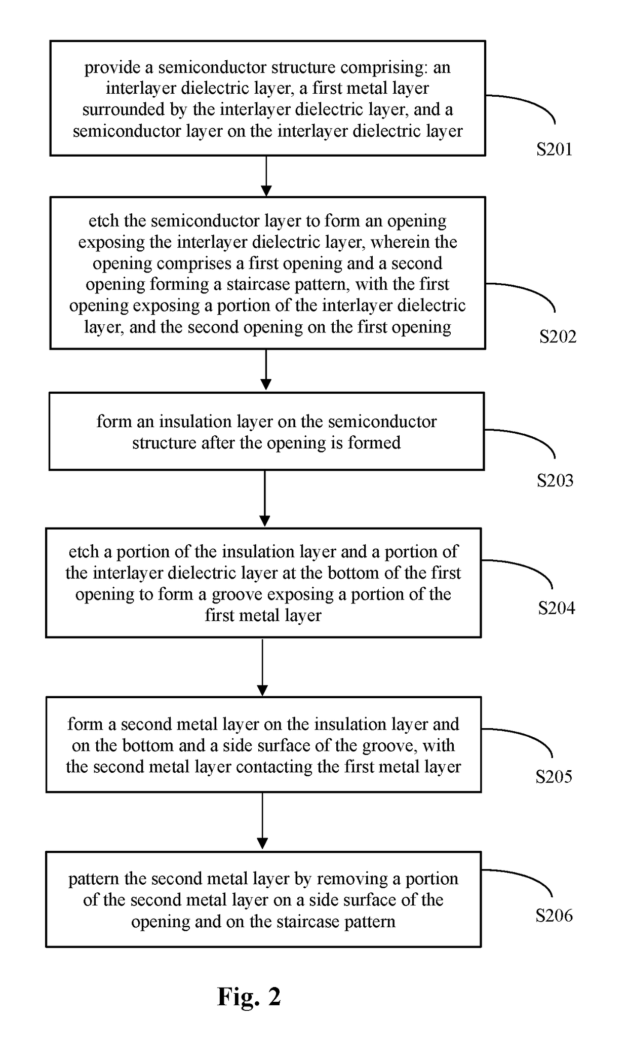
[0050]Example embodiments of the inventive concept are described with reference to the accompanying drawings. As those skilled in the art would realize, the described embodiments may be modified in various ways without departing from the spirit or scope of the inventive concept. Embodiments may be practiced without some or all of these specified details. Well known process steps and / or structures may not be described in details, in the interest of clarity.

[0051]The drawings and descriptions are illustrative and not restrictive. Like reference numerals may designate like (e.g., analogous or identical) elements in the specification. To the extent possible, any repetitive description will be minimized.

[0052]Relative sizes and thicknesses of elements shown in the drawings are chosen to facilitate description and understanding, without limiting the inventive concept. In the drawings, the thicknesses of some layers, films, panels, regions, etc., may be exaggerated for clarity.

[0053]Embodi...


PUM


Abstract

A semiconductor device and its manufacturing method are presented. The manufacturing method includes: providing a semiconductor structure comprising: an interlayer dielectric layer, a first metal layer surrounded by the interlayer dielectric layer, and a semiconductor layer on the interlayer dielectric layer; etching the semiconductor layer to form an opening exposing the interlayer dielectric layer, wherein the opening comprises a first opening and a second opening on the first opening; forming an insulation layer on the semiconductor structure; etching the insulation layer and the interlayer dielectric layer at the bottom of the first opening to form a groove exposing a portion of the first metal layer; forming a second metal layer on the insulation layer and on the bottom and a side surface of the groove; and patterning the second metal layer. The second metal layer in this inventive concept can be removed more completely than conventional methods.

Description

CROSS-REFERENCE TO RELATED APPLICATION[0001]This application claims priority to and benefit of Chinese Patent Application No. 201710350090.0 filed on May 18, 2017, which is incorporated herein by reference in its entirety.BACKGROUND(a) Field of the Invention[0002]This inventive concept relates generally to semiconductor techniques, and more specifically, to a semiconductor device and its manufacturing method.(b) Description of the Related Art[0003]The manufacture of Backside Illuminated Complementary Metal-Oxide-Semiconductor Image Sensor (BSI CIS) is a complicated process. Typically, after a device process is completed, a device wafer is bonded to a handle wafer, and a patterned liner layer (e.g., an aluminum layer) is formed for metal wire connection. Major procedures in a BSI CIS manufacturing process include a procedure to etch silicon to form an opening and a procedure to etch an interlayer dielectric layer to form a groove.[0004]FIG. 1A shows a structure in a conventional manu...

Claims


Application Information

Patent Timeline
IPC IPC(8): H01L23/00
CPCH01L24/05H01L24/03H01L2224/0345H01L2224/03614H01L2224/03622H01L2224/04042H01L2224/05018H01L2224/05027H01L2224/05124H01L27/14687H01L27/14632H01L27/1464H01L21/3086H01L27/14636H01L27/14683
Inventor WU, YOUZHU, JUN
Owner SEMICON MFG INT (SHANGHAI) CORP
Why Eureka
Eureka Blog
Learn More