
Pixel array, display panel and curved display panel

a technology of display panel and array, which is applied in the field of pixel array, display panel and curved display panel, can solve the problems of unfavorable display quality and deterioration of display quality of certain regions of curved display panel

Active Publication Date: 2018-11-29
AU OPTRONICS CORP
View PDF48 Cites 2 Cited by
  • Summary
  • Abstract
  • Description
  • Claims
  • Application Information

AI Technical Summary

Benefits of technology

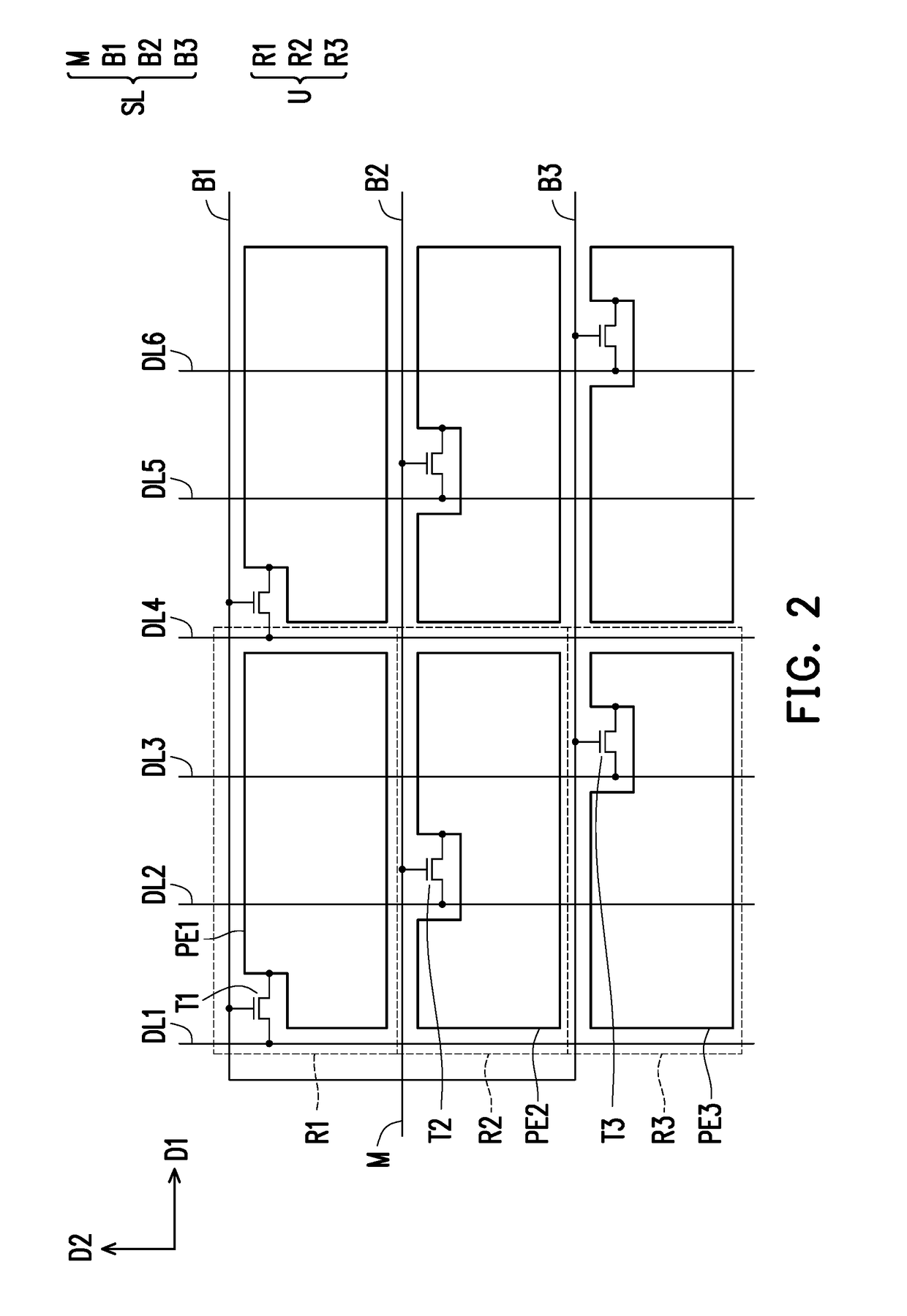
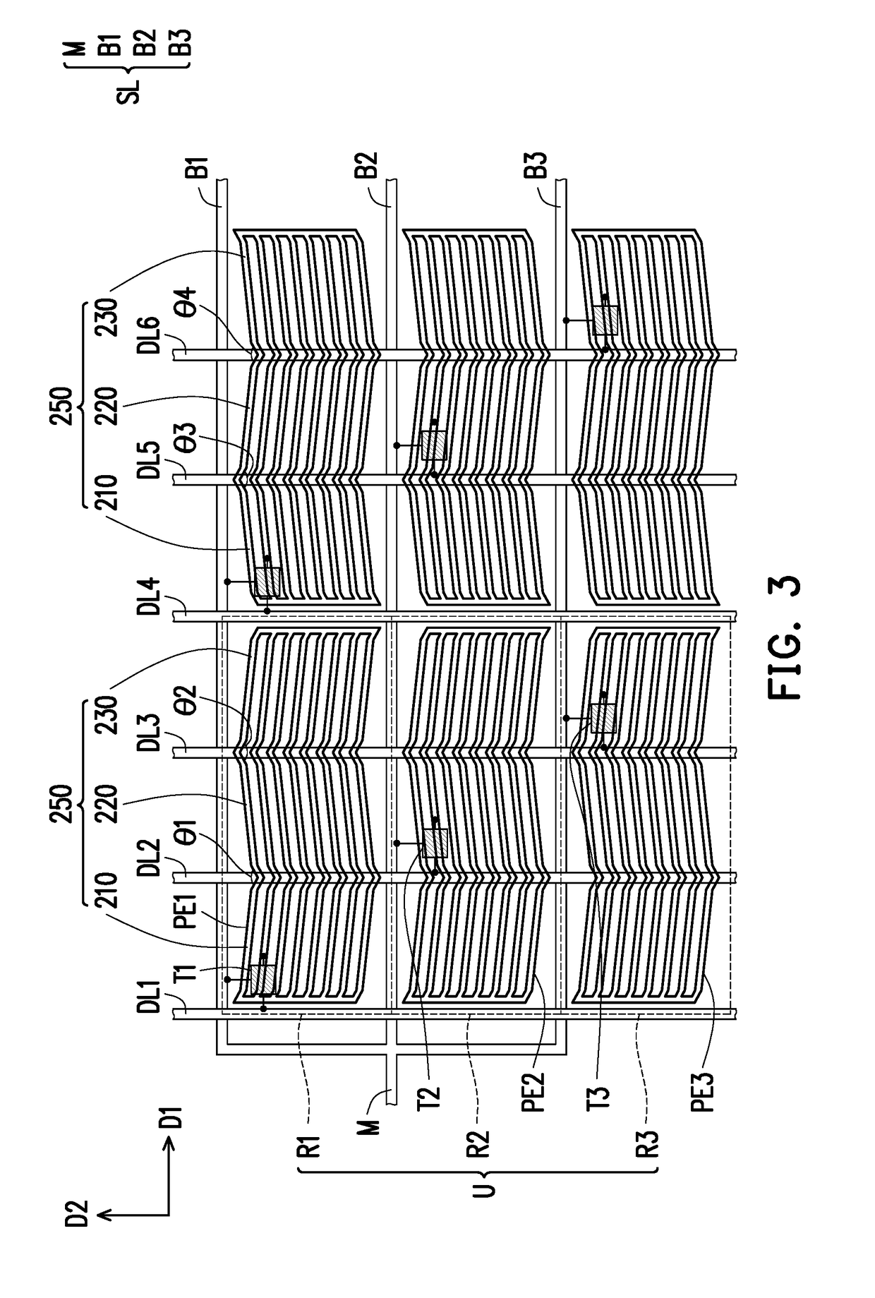
The present invention provides a pixel array with a scan line system that includes a main scan line, a first branch scan line, and a second branch scan line. The first and second data lines are overlapped with both the first and second pixel electrodes. This arrangement makes it easier to select different gate driving chips. Additionally, the use of curved display panels can help alleviate issues related to misalignment between pixel unit sets and devices on the other substrate. Ultimately, these features contribute to improved display quality.

Problems solved by technology

However, after the two substrates are bent, the components on the two substrates may be misaligned, such that the display quality of certain regions on the curved display panel may be deteriorated.
In addition, in the curved display panel, the issue of unfavorable display quality resulting from the misalignment of the pixel unit sets on the pixel array and the devices on the other substrate can be resolved to a great extent.

Method used


Image

  • Pixel array, display panel and curved display panel
  • Pixel array, display panel and curved display panel
  • Pixel array, display panel and curved display panel

Examples


Embodiment Construction

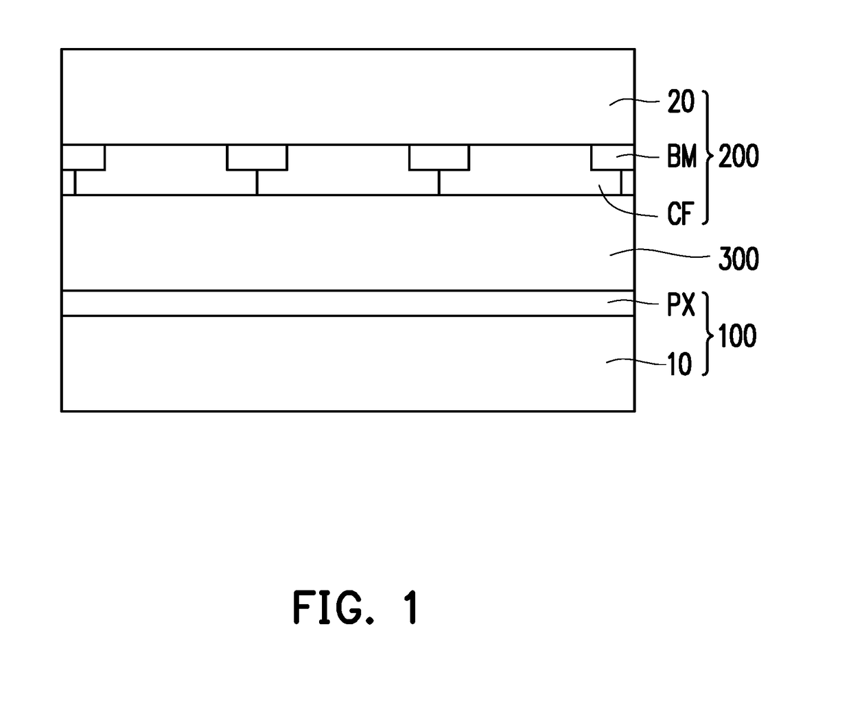
[0019]FIG. 1 is a schematic cross-sectional view illustrating a display panel according to an embodiment of the disclosure. In the present embodiment, the display panel includes a first substrate 10, a pixel array PX, a second substrate 20, and a color filter layer CF. With reference to the present embodiment, the display panel further includes a light shielding pattern layer BM and a display medium 300. Here, the first substrate 10 and the pixel array PX constitute the pixel array substrate 100, and the second substrate 20, the light shielding pattern layer BM, and the color filter layer CF constitute a color filter substrate 200. It should be mentioned that the color filter layer CF is not limited to be formed on the second substrate 20; in another embodiment of the disclosure, the color filter layer CF may be formed on the first substrate 10, so as to form a color-filter-on-array (COA) structure.

[0020]The first substrate 10 may be made of glass, quartz, or an organic polymer. The...


PUM

PropertyMeasurementUnit
angleaaaaaaaaaa
angleaaaaaaaaaa
θaaaaaaaaaa

Abstract

A pixel array includes pixel unit sets each including a substrate having first and second pixel regions, a scan line, first and second data lines extending along a second direction, first and second active devices respectively in the first and second pixel regions, and first and second pixel electrodes respectively located in the first and second pixel regions and electrically connected to the first and second active devices, respectively. The scan line includes a main scan line and first and second branch scan lines (connected to the main scan line) extending along a first direction. The first active device is electrically connected to the first branch scan line and the first data line. The second active device is electrically connected to the second branch scan line and the second data line. At least one of the first and second data lines is overlapped with the first and second pixel electrodes.

Description

CROSS-REFERENCE TO RELATED APPLICATION[0001]This application is a divisional of and claims priority benefit of U.S. patent application Ser. No. 15 / 232,793, filed on Aug. 9, 2016, now allowed, which claims the priority benefit of Taiwan application serial no. 104125895, filed on Aug. 10, 2015. The entirety of each of the above-mentioned patent applications is hereby incorporated by reference herein and made a part of this specification.FIELD OF DISCLOSURE[0002]The disclosure relates to a pixel array, a display panel, and a curved display panel.DESCRIPTION OF RELATED ART[0003]With the advancement of science and technology, display technologies have also been continuously developing. Light, thin, compact, and slim flat panel displays (FPD) have gradually replaced the conventional cathode ray tube (CRT) displays. At present, the FPD characterized by compactness and slimness has been further employed on non-planar surfaces of various buildings or electronic equipment. In order to be adap...

Claims


Application Information

Patent Timeline
Patent Type & Authority Applications(United States)
IPC IPC(8): G02F1/1362G02F1/1343H01L27/12G02F1/1335
CPCG02F2001/136295H01L27/1262G02F2001/134345G02F1/136286H01L27/124G02F1/133512G02F1/134336G02F1/134309G02F1/167H01L27/1218G02F1/134345G02F1/136295
Inventor LIN, CHUN-FENGHSIEH, YAO-ANKUO, YU-PINGCHENG, CHING-SHENG
Owner AU OPTRONICS CORP
Learn More