Semiconductor structure and fabrication method thereof

a semiconductor structure and semiconductor technology, applied in the direction of semiconductor devices, basic electric elements, electrical appliances, etc., can solve the problems of difficult to match the difference between the requirements of the oxidation process on the storage region and the requirements of the oxidation process on the peripheral region, and the performance of the semiconductor structure having the memory device is not as desired

Active Publication Date: 2018-11-29
SEMICON MFG INT (SHANGHAI) CORP +1
View PDF1 Cites 9 Cited by
  • Summary
  • Abstract
  • Description
  • Claims
  • Application Information

AI Technical Summary

Problems solved by technology

However, it is difficult to match the difference between the requirements of the oxidation process on the storage region and the requirements of

Method used


Image

  • Semiconductor structure and fabrication method thereof
  • Semiconductor structure and fabrication method thereof
  • Semiconductor structure and fabrication method thereof

Examples


Embodiment Construction

[0014]Reference will now be made in detail to exemplary embodiments of the disclosure, which are illustrated in the accompanying drawings. Wherever possible, the same reference numbers will be used throughout the drawings to refer to the same or like parts.

[0015]FIGS. 1-2 illustrate structures corresponding to certain stages during a process for forming a semiconductor structure.

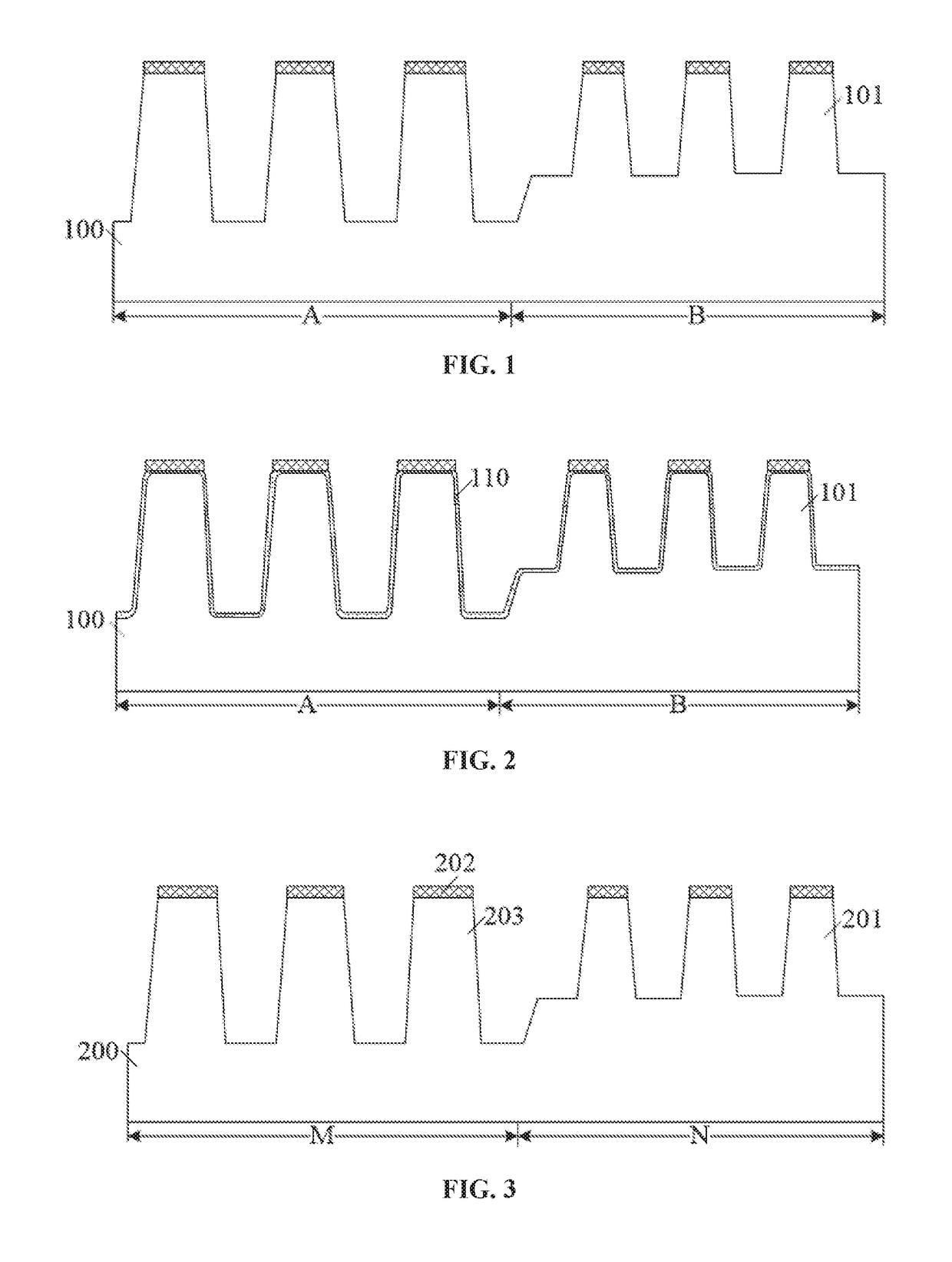
[0016]As shown in FIG. 1, the fabrication process includes providing a semiconductor substrate 100. The semiconductor substrate 100 has a peripheral region “A” and a storage region “B”. A plurality of fins 101 are formed on the semiconductor substrate 100 in the peripheral region “A” and the storage region “B”.

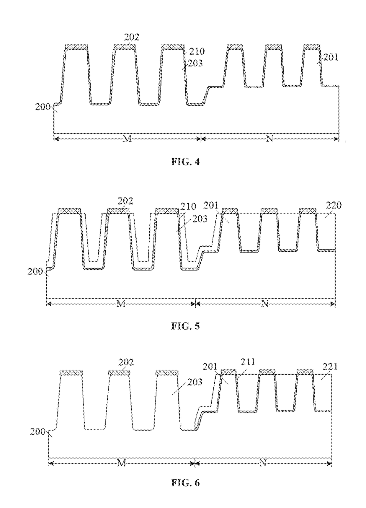
[0017]Further, as shown in FIG. 2, the fabrication process also includes performing an oxidation process on the fins 101 to form an oxide layer 110 on the surface of the fins 101.

[0018]The top surfaces of the fins 101 and the side surfaces of the fins 101 may have rounded corners. The oxidation process...


PUM


Abstract

Semiconductor structures and fabrication methods thereof are provided. An exemplary fabrication process includes providing a semiconductor substrate having a first region and a second region and having a plurality of first fins in the first region and a plurality of second fins in the second region; performing a first oxidation process on the first fins to form a first oxide layer on surfaces of the first fins and to cause corners between top surfaces and side surface of the first fins to form first rounded corners; and performing a second oxidation process on the second fins to form a second oxide layer on surfaces of the second fins and to cause corners between top surfaces and side surface of the second fins to form second rounded corners. A radius of curvature of the first rounded corner is different from a radius of curvature of the second rounded corner.

Description

CROSS-REFERENCES TO RELATED APPLICATIONS[0001]This application claims the priority of Chinese patent application No. 201710372717.2, filed on May 24, 2017, the entirety of which is incorporated herein by reference.FIELD OF THE DISCLOSURE[0002]The present disclosure generally relates to the field of semiconductor manufacturing technologies and, more particularly, relates to semiconductor structures and fabrication methods thereof.BACKGROUND[0003]With the continuous development of semiconductor technologies, semiconductor devices have been developed toward high integration level with high quality. The critical dimension (CD) of the semiconductor devices has been correspondingly reduced. Reducing the critical dimension of the semiconductor devices allows more transistors to be formed on one chip. Accordingly, the performance of the semiconductor devices is improved.[0004]In the field of memory devices, with the development of information technologies, the amount of the information have...

Claims


Application Information

Patent Timeline
IPC IPC(8): H01L29/78H01L21/02H01L21/762H01L27/115H01L29/66
CPCH01L29/785H01L21/02236H01L21/76202H01L21/02274H01L27/115H01L29/66795H01L21/823412H01L21/823431H01L27/105H10B99/00H01L21/76229H01L21/76232H01L21/02255H01L29/7854H01L27/0886H10B41/42H10B43/40H10B69/00
Inventor HU, JIAN QIANG
Owner SEMICON MFG INT (SHANGHAI) CORP
Why Eureka
Try Eureka