Integrated circuit device and method of manufacturing the same

Active Publication Date: 2018-12-06
SAMSUNG ELECTRONICS CO LTD
View PDF13 Cites 8 Cited by
  • Summary
  • Abstract
  • Description
  • Claims
  • Application Information

AI Technical Summary

Benefits of technology

[0009]The integrated circuit device according to an exemplary embodiment of the present inventive concept may have a structure in which the undercut region formed in the interface region is filled by a buried pattern so a metal contamination source may be prevented from remaining in the interface region. Thus, while dense and fine structures such as a plurality of bit line structures are formed in the cell array region, contamination of the minute structures by a metal contamination source may be reduced or eliminated, and degradation of electrical characteristics and reliability of the integra

Problems solved by technology

Contamination by impurities such as metal particles during a manufacturing process of a compact

Method used


Image

  • Integrated circuit device and method of manufacturing the same
  • Integrated circuit device and method of manufacturing the same
  • Integrated circuit device and method of manufacturing the same

Examples


Embodiment Construction

[0021]Exemplary embodiments of the present inventive concept will be described below in more detail with reference to the accompanying drawings. In this regard, the exemplary embodiments may have different forms and should not be construed as being limited to the exemplary embodiments of the present inventive concept described herein. Like reference numerals may refer to like elements throughout the specification and drawings.

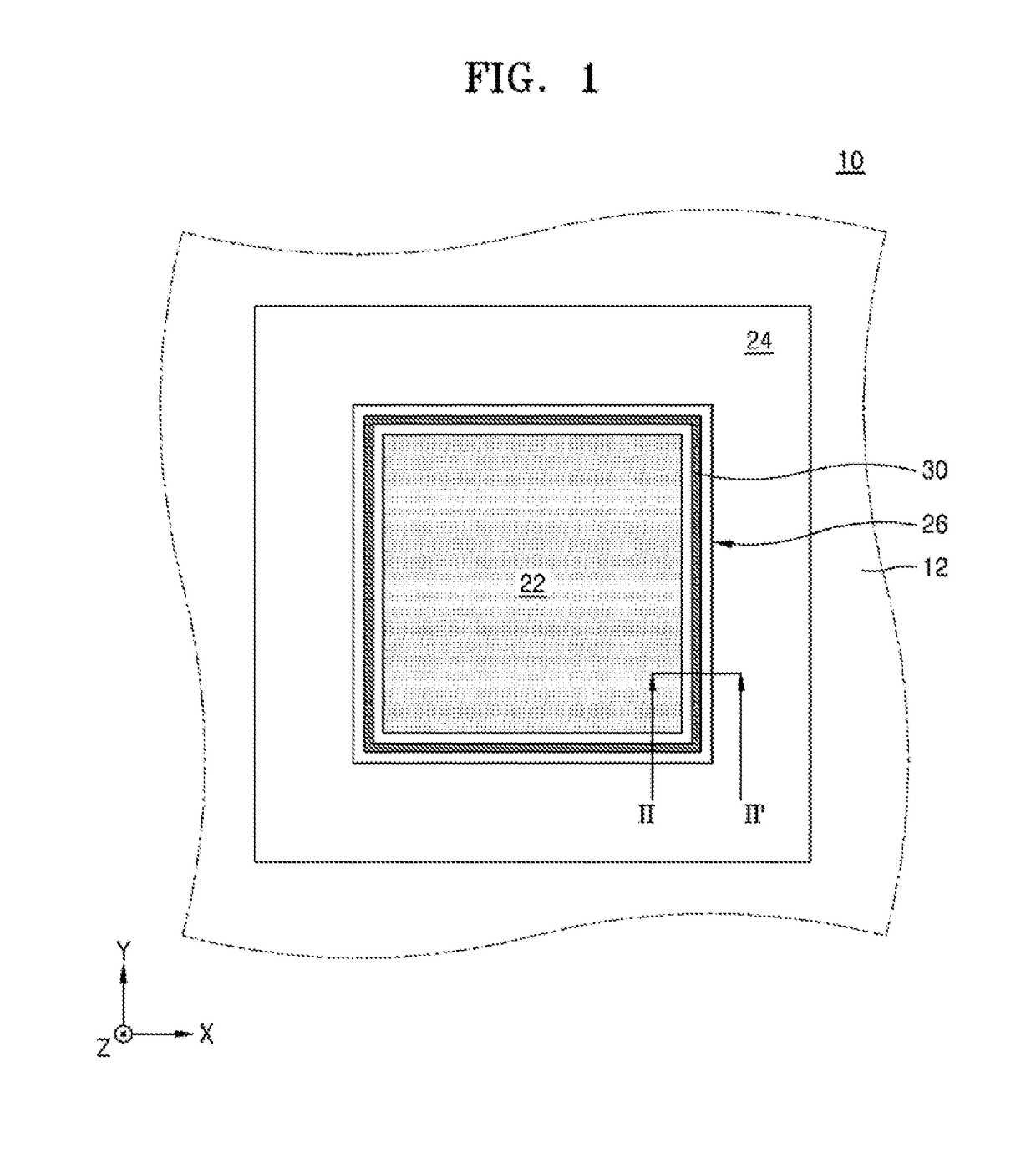
[0022]FIG. 1 is a plan view illustrating a schematic structure of an integrated circuit device according to an exemplary embodiment of the present inventive concept.

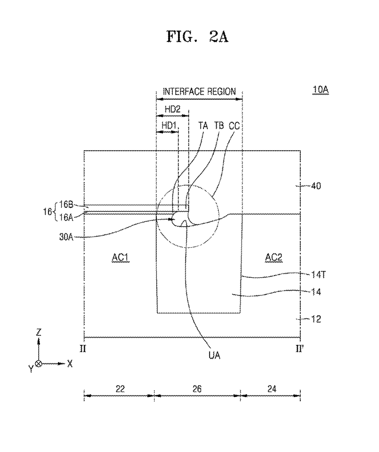
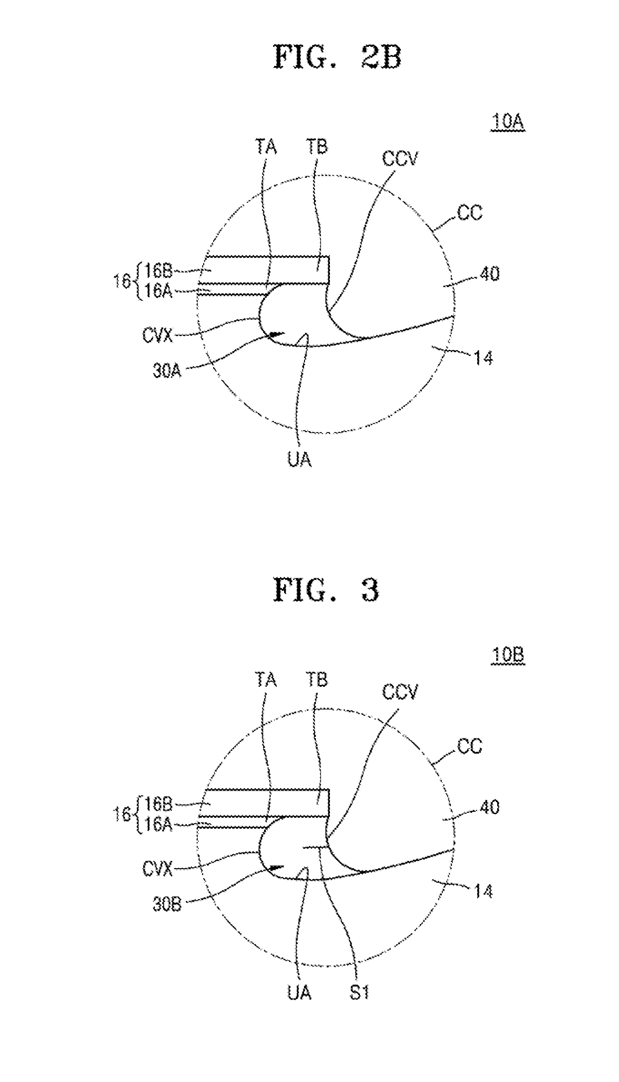
[0023]Referring to FIG. 1, an integrated circuit device 10 may include a substrate 12 including a first region 22, a second region 24 surrounding the first region 22, and an interface region 26 positioned between the first region 22 and the second region 24 along a direction parallel to an upper surface of the substrate 12.

[0024]The substrate 12 may include a semiconductor element such as Si or Ge o...


PUM


Abstract

An integrated circuit device includes a substrate having a first region and a second region separated from each other along a direction parallel to an upper surface of the substrate. An interface device isolation layer fills an interface trench in an interface region between the first region and the second region and defines a portion of a first active area positioned in the first region and a portion of a second active area positioned in the second region. An insulation pattern extends from the first region to an upper portion of the interface device isolation layer. The insulation pattern covers the first active area and at least a portion of the interface device isolation layer. The insulation pattern defines an undercut area on an upper surface of the interface device isolation layer. A buried pattern substantially fills the undercut region.

Description

CROSS-REFERENCE TO RELATED APPLICATION[0001]This application claims priority under 35 U.S.C. § 119 to Korean Patent Application No. 10-2017-0067634, filed on May 31, 2017, in the Korean Intellectual Property Office, the disclosure of which is incorporated by reference herein in its entirety.TECHNICAL FIELD[0002]Exemplary embodiments of the present inventive concept relate to an integrated circuit device, and more particularly to a method of manufacturing the same.DISCUSSION OF RELATED ART[0003]With the development of electronic technology, down-scaling of integrated circuit devices has rapidly progressed, and integrated circuit devices are becoming more compact. Contamination by impurities such as metal particles during a manufacturing process of a compact integrated circuit device may reduce performance and yield of such integrated circuit devices.SUMMARY[0004]An exemplary embodiment of the present inventive concept provides an integrated circuit device in which contamination by im...

Claims


Application Information

Patent Timeline
IPC IPC(8): H01L29/06H01L27/108H01L21/762
CPCH01L29/0649H01L27/10814H01L27/10897H01L21/76232H01L27/10894G11C11/4085H10B43/30H10B12/315H10B12/50H10B12/09H01L21/7624H01L21/76838H01L21/76237H01L21/7681
Inventor YOON, CHAN-SICLEE, HO-INLEE, KI-SEOKPARK, JE-MIN
Owner SAMSUNG ELECTRONICS CO LTD
Why Eureka
Try Eureka