Thin film transistor, TFT substrate, and display panel

Active Publication Date: 2018-12-13
SHENZHEN CHINA STAR OPTOELECTRONICS SEMICON DISPLAY TECH CO LTD
View PDF3 Cites 0 Cited by
  • Summary
  • Abstract
  • Description
  • Claims
  • Application Information

AI Technical Summary

Benefits of technology

[0008]The adoption of the present disclosure will bring some benefits. Compared with the related art, the present disclosure provides a TFT, a TFT substrate, and a display panel, and a gate, a sourc

Problems solved by technology

Such a structure is disfavored when the gate sid

Method used


Image

  • Thin film transistor, TFT substrate, and display panel
  • Thin film transistor, TFT substrate, and display panel
  • Thin film transistor, TFT substrate, and display panel

Examples


Example

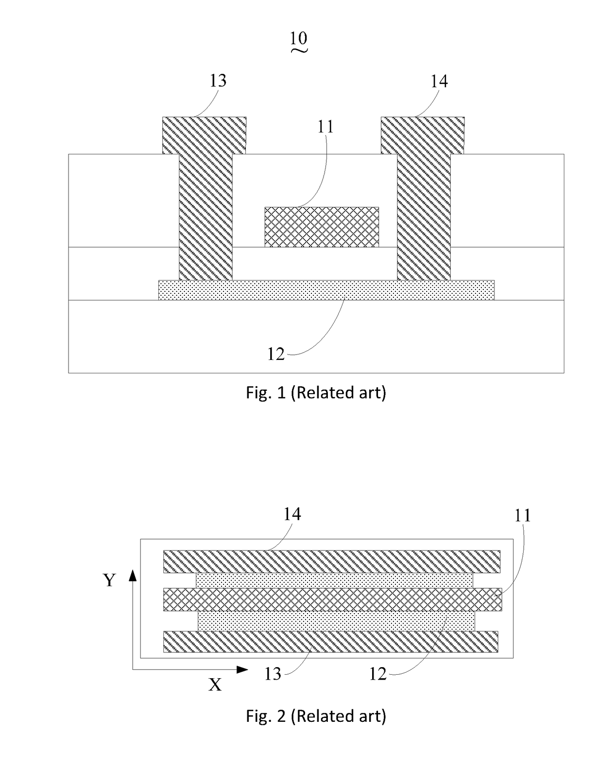
[0019]The invention is described below in detail with reference to the accompanying drawings, wherein like reference numerals are used to identify like elements illustrated in one or more of the figures thereof, and in which exemplary embodiments of the invention are shown. This invention may, however, be embodied in many different forms and should not be construed as limited to the particular embodiments set forth herein. Rather, these embodiments are provided so that this disclosure will be thorough and complete, and will fully convey the scope of the invention to those skilled in the art. The drawings illustrate embodiments of the invention and, together with the description, serve to explain the principles of the invention.

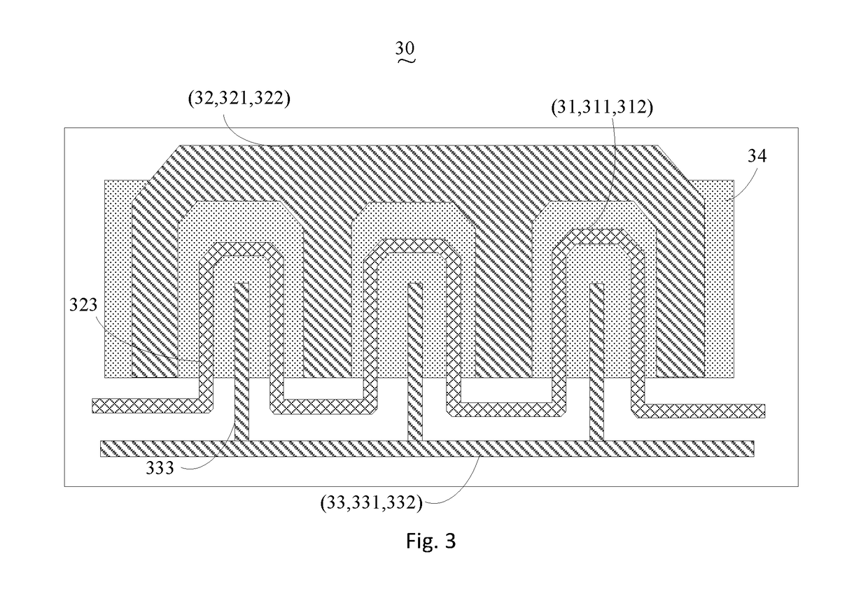
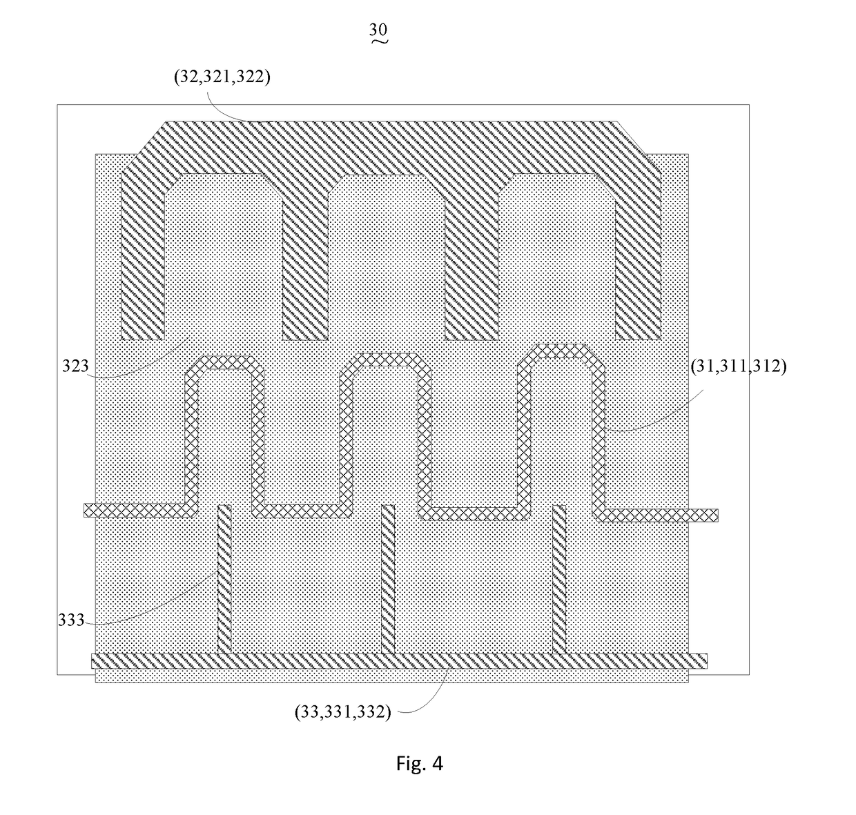
[0020]FIG. 3 illustrates a schematic diagram of the structure of a thin film transistor (TFT) 30 in an embodiment of the present disclosure. The TFT 30 includes a gate 31, a source 33, a drain 32, and a semiconductor layer 34. The source 33 is a first bending ...


PUM


Abstract

A thin film transistor, a TFT substrate, and a display panel are provided. The TFT includes a gate, a source, and a drain. The source is a first bending structure. The drain is a second bending structure. The gate is a third bending structure. The first bending structure of the source and the second bending structure of the drain are arranged opposite. The third bending structure of the gate is arranged between the first bending structure of the source and the second bending structure of the drain. The present disclosure facilitates fabrication of a narrow bezel of a display panel.

Description

BACKGROUND1. Field of the Disclosure[0001]The present disclosure relates to the field of display, and more particularly, to a thin film transistor (TFT), a TFT substrate, and a display panel.2. Description of Related Art[0002]A gate driver on array (GOA) is a shift register formed by a plurality of thin film transistors (TFTs). The gate driver is fabricated on an array glass substrate so the space for gate driver bonding is spared, which is good for fabrication of a narrow bezel on a gate side.[0003]Please refer to FIG. 1 illustrating a cross-sectional view of a gate 11 arranged on a top gate indium gallium zinc oxide-TFT (top gate IGZO-TFT). The gate 11 of the TFT 10 is arranged is arranged on a semiconductor layer 12. A source 13 and a drain 14 are both electrically connected to the semiconductor layer 12. The TFT 10 has advantages of high mobility and small parasitic capacitance so a good waveform with small resistor-capacitor (RC) delay can be output, which is one of the current...

Claims


Application Information

Patent Timeline
IPC IPC(8): G02F1/1345H01L27/12H01L29/786H01L29/423H01L29/417G02F1/1368
CPCG02F1/13454H01L27/1225H01L29/7869H01L29/42384H01L29/41733G02F1/1368G02F2202/10G02F2201/124G09G3/3677G09G2310/0286
Inventor SHI, LONGQIANGCHEN, SHU-JHIH
Owner SHENZHEN CHINA STAR OPTOELECTRONICS SEMICON DISPLAY TECH CO LTD
Why Eureka
Try Eureka